TDA3661 查看數據表(PDF) - Philips Electronics
零件编号
产品描述 (功能)
比赛名单
TDA3661 Datasheet PDF : 16 Pages
| |||
Philips Semiconductors
Very low dropout voltage/quiescent current
adjustable voltage regulator
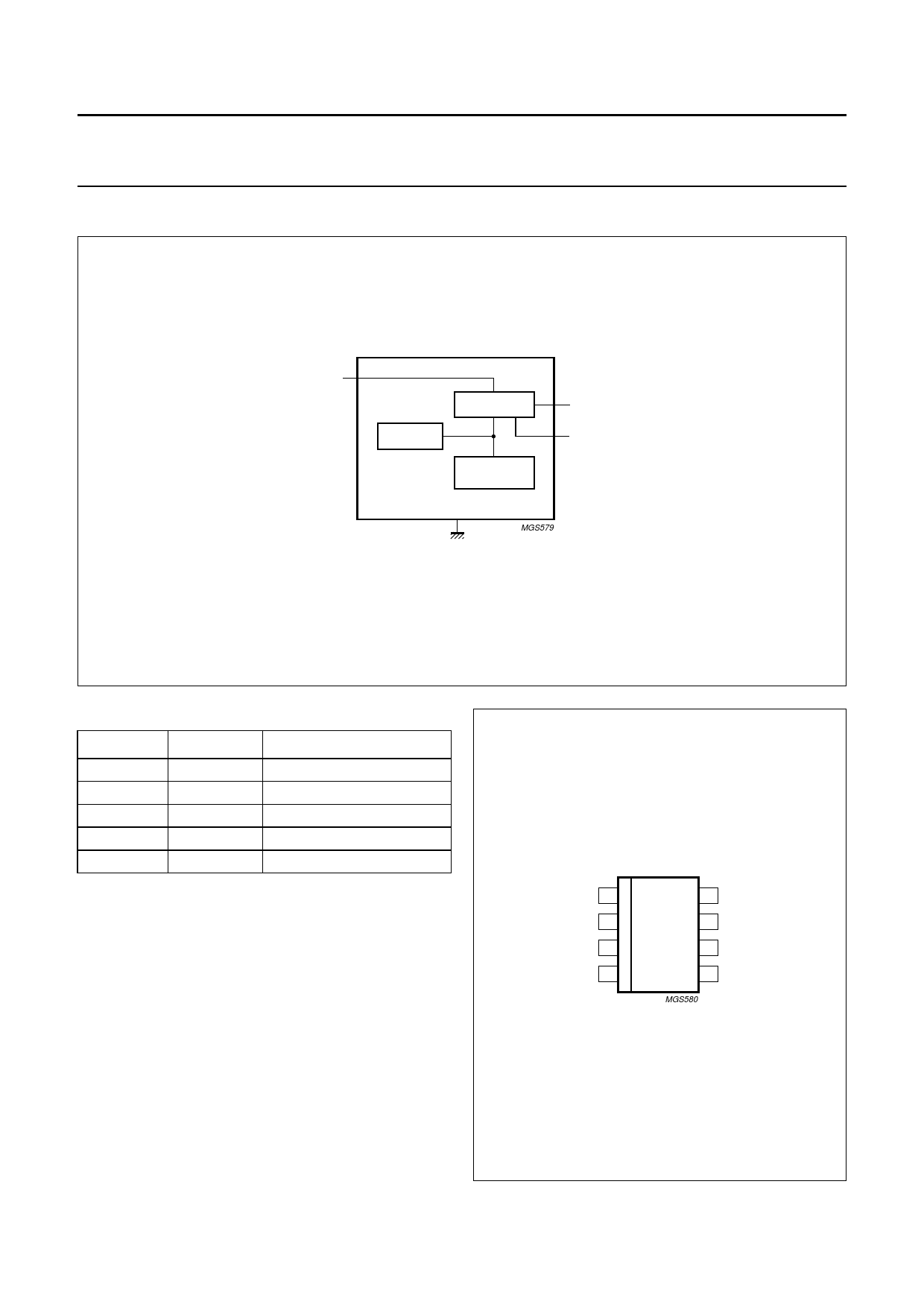
BLOCK DIAGRAM
Preliminary specification
TDA3661
handbook,
halfpage
VP
8
BAND GAP
1
REGULATOR
5
REG
ADJ
TDA3661
THERMAL
PROTECTION
2, 3, 6, 7
GND
MGS579
Fig.1 Block diagram.
PINNING
SYMBOL
PIN
DESCRIPTION
REG
GND
n.c.
ADJ
VP
1
regulator output
2, 3, 6 and 7 ground; note 1
4
not connected
5
feedback input
8
supply voltage
Note
1. All GND pins are connected to the lead frame and can
also be used to reduce the total thermal resistance
Rth(j-a) by soldering these pins to a ground plane.
The ground plane on the top side of the PCB acts like
a heat spreader.
handbook, halfpage
REG 1
GND 2
GND 3
n.c. 4
8 VP
7 GND
TDA3661
6 GND
5 ADJ
MGS580
2000 Feb 01
Fig.2 Pin configuration.
3
Share Link: 