DG4051A 查看數據表(PDF) - Vishay Semiconductors
零件编号
产品描述 (功能)
比赛名单
DG4051A Datasheet PDF : 16 Pages
| |||
DG4051A, DG4052A, DG4053A
Vishay Siliconix
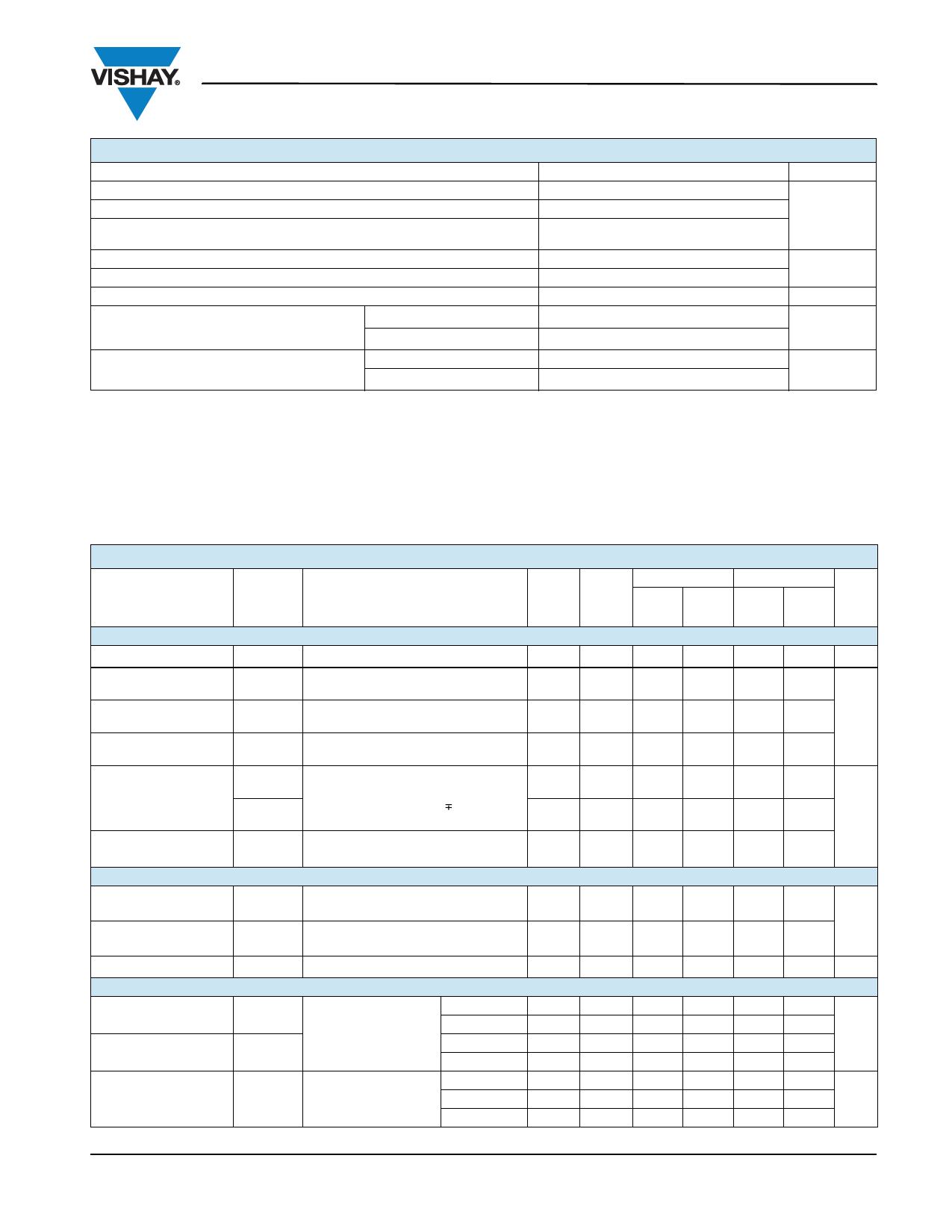
ABSOLUTE MAXIMUM RATINGS TA = 25 °C, unless otherwise noted
Parameter
Limit
Unit
V+ to V-
14
GND to V-
Digital Inputsa, VS, VD
7
V
(V-) - 0.3 to (V+) + 0.3
or 30 mA, whichever occurs first
Continuous Current (Any terminal)
Peak Current, S or D (Pulsed 1 ms, 10 % duty cycle)
30
mA
100
Storage Temperature
- 65 to 150
°C
Power Dissipationb
16-Pin TSSOPc
16-Pin miniQFNd, e
450
mW
525
Thermal Resistanceb
16-Pin TSSOP
16-Pin miniQFNe
178
°C/W
152
Notes:
a. Signals on SX, DX, or INX exceeding V+ or V- will be clamped by internal diodes. Limit forward diode current to maximum current ratings.
b. All leads welded or soldered to PC board.
c. Derate 5.6 mW/°C above 70 °C.
d. Derate 6.6 mW/°C above 70 °C.
e. Manual soldering with iron is not recommended for leadless components. The miniQFN-16 is a leadless package. The end of the lead terminal
is exposed copper (not plated) as a result of the singulation process in manufacturing. A solder fillet at the exposed copper lip cannot be
guaranteed and is not required to ensure adequate bottom side solder interconnection.
SPECIFICATIONS FOR DUAL SUPPLIES
Parameter
Analog Switch
Symbol
Test Conditions
Unless Otherwise Specified
VIN(A,
VCC = + 5 V, VEE
B, C and ENABLE) =
=-5V
2.0 V, 0.8
Va
Analog Signal Rangee VANALOG
On-Resistance
RON
IS = 1 mA, VD = - 3 V, 0 V, + 3 V
On-Resistance Match
RON
IS = 1 mA, VD = ± 3 V
On-Resistance
Flatness
RFLATNESS
IS = 1 mA, VD = - 3 V, 0 V, + 3 V
Switch Off
Leakage Current
IS(off)
ID(off)
V+ = 5.5 V, V- = - 5.5 V,
VD = ± 4.5 V, VS = 4.5 V
Channel On
Leakage Current
Digital Control
Input Current, VIN Low
ID(on)
IIL
Input Current, VIN High
IIH
Input Capacitancee
CIN
Dynamic Characteristics
Off Isolation
OIRR
Channel-to-Channel
Crosstalk
XTALK
Bandwith, 3 dB
BW
V+ = 5.5 V, V- = - 5.5 V,
VS = VD = ± 4.5 V
VIN(A, B, C and ENABLE)
under test = 0.8 V
VIN(A, B, C and ENABLE)
under test = 2.0 V
f = 1 MHz
RL = 50 , CL = 1 pF
RL = 50
f = 10 MHz
f = 100 MHz
f = 10 MHz
f = 100 MHz
DG4051A
DG4052A
DG4053A
Temp.b
Full
Room
Full
Room
Full
Room
Full
Room
Full
Room
Full
Room
Full
Full
Full
Room
Room
Room
Room
Room
Room
Room
Room
- 40 °C to 125 °C - 40 °C to 85 °C
Typ.c Min.d Max.d Min.d Max.d
-5
5
-5
5
66
100
100
125
118
3
6
6
10
8
12
16
16
20
18
± 0.02 - 1
1
-1
1
- 50
50
-5
5
± 0.02 - 1
1
-1
1
- 50
50
-5
5
± 0.02 - 1
1
-1
1
- 50
50
-5
5
0.01
-1
1
-1
1
0.01
-1
1
-1
1
3.4
67
46
67
47
330
450
730
Unit
V
nA
µA
pF
dB
MHz
Document Number: 69828
S10-1383-Rev. E, 21-Jun-10
www.vishay.com
3
Share Link: 