DG9451 查看數據表(PDF) - Vishay Semiconductors
零件编号
产品描述 (功能)
比赛名单
DG9451 Datasheet PDF : 13 Pages
| |||
www.vishay.com
DG9451, DG9453
Vishay Siliconix
8-Channel, Triple 2-Channel Multiplexers
DESCRIPTION
The DG9451, and DG9453 are high precision single and
dual supply CMOS analog multiplexers. DG9451 is an
8-channel multiplexer, and the DG9453 is a triple 2-channel
multiplexer or triple SPDT.
Designed to operate from a +2.7 V to +12 V single supply or
from a ± 2.5 V to ± 5 V dual supplies, the DG9451, and
DG9453 are fully specified at +12 V, +5 V and ± 5 V. All
control logic inputs have guaranteed 1.4 V high limit when
operating from +5 V or ± 5 V supplies and 1.65 V when
operating from a +12 V supply.
The DG9451, and DG9453 are precision multiplexers of low
leakage, low charge injection, and low parasitic
capacitance. They conduct equally well in both directions,
offer rail to rail analog signal handling and can be used both
as multiplexers as well as de-multiplexers.
The DG9451, and DG9453 operating temperature is
specified from -40 °C to +85 °C and are available in 16 pin
TSSOP and the ultra compact 1.8 mm x 2.6 mm miniQFN16
packages.
FEATURES
• +2.7 V to +12 V single supply operation
± 2.5 V to ± 5 V dual supply operation
• Fully specified at +12 V, +5 V, ± 5 V
• Low charge injection (< 0.5 pC typ.)
• High bandwidth: 270 MHz
• Low switch capacitance (Cs(off) 1 pF typ.)
• Good isolation and crosstalk performance
(typ. -44 dB at 100 MHz)
• MiniQFN16 package (1.8 mm x 2.6 mm)
• Material categorization: for definitions of compliance
please see www.vishay.com/doc?99912
APPLICATIONS
• Data acquisition
• Medical and healthcare devices
• Control and automation equipments
• Test instruments
• Touch panels
• Consumer
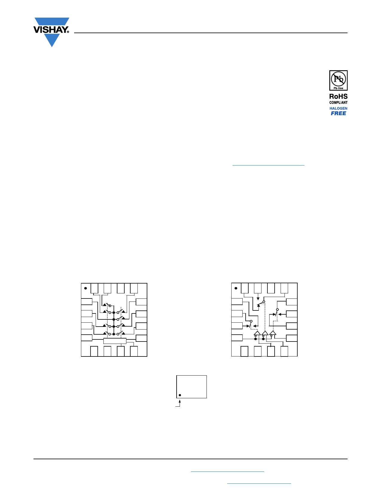
FUNCTIONAL BLOCK DIAGRAM AND PIN CONFIGURATION
DG9451
mQFN-16
X6
X4
VCC
X2
16
15
14
13
DG9453
mQFN-16
Y0
Y1
VCC
Y
16
15
14
13
X1
X7 2
12 X1
11 X0
Z1 1
Z
2
12 X
11 X1
X5 3
ENABLE 4
Logic
5
6
77
VEE
GND
C
Top View
10 X3
9A
8
B
Z0
3
ENABLE
4
10 X0
9A
5
6
77
8
VEE
GND
C
B
Top View
Yxx
Pin 1
Device Marking: Yxx for DG9451
(miniQFN16) 4xx for DG9453
xx = Date/Lot Traceability Code
S14-2340-Rev. C, 08-Dec-14
1
Document Number: 65020
For technical questions, contact: powerictechsupport@vishay.com
THIS DOCUMENT IS SUBJECT TO CHANGE WITHOUT NOTICE. THE PRODUCTS DESCRIBED HEREIN AND THIS DOCUMENT
ARE SUBJECT TO SPECIFIC DISCLAIMERS, SET FORTH AT www.vishay.com/doc?91000
Share Link: 