DS21S07AE-TR 查看數據表(PDF) - Maxim Integrated
零件编号
产品描述 (功能)
比赛名单
DS21S07AE-TR Datasheet PDF : 8 Pages
| |||
DS21S087A
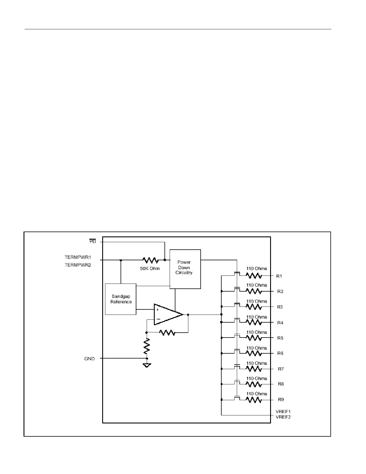
FUNCTIONAL DESCRIPTION
The DS21S07A consists of a bandgap reference, buffer amplifier, and nine termination resistors
(Figure 1). The bandgap reference circuit produces a precise 2.55V level that is fed to a buffer amplifier.
The buffer produces a 2.85V level and can source at least 24mA into each of the termination resistors
when the signal line is low (active). When the driver for a given signal line turns off, the terminator pulls
the signal line to 2.85V (quiescent state). To handle actively negated SCSI signals, the buffer can sink at
least 200mA, and VREF will move less than 60mV. When all lines settle in the quiescent state, the
regulator consumes about 2.5mA. When the DS21S07A is put into power-down mode by bringing PD
low, the power-down circuitry turns off the transistors on each signal line. This isolates the DS21S07A
from the signal lines and effectively removes it from the circuit. The power-down pin (PD) has an internal
50kΩ pullup resistor. To place the DS21S07A into an active state, the PD pin should be left open
circuited. When installed on disk drives or RAID system components, the DS21S07A will not affect the
SCSI bus during a hot plug operation.
To ensure proper operation, both the TERMPWR1 and TERMPWR2 pins must be connected to the SCSI
bus TERMPWR line and both the VREF1 and VREF2 pins must be tied together externally. Each
DS21S07A requires a 4.7µF capacitor connected between the VREF pins and ground. Figure 2 details a
typical SCSI bus configuration. In an 8-bit-wide SCSI bus arrangement (“A” Cable), two DS21S07A’s
would be needed at each end of the SCSI cable to terminate the 18 active signal lines. In a 16-bit-wide
SCSI bus arrangement (“P” Cable), three DS21S07A’s would be needed at each end of the SCSI cable to
terminate the 27 active signal lines.
Figure 1. DS21S087A Block Diagram
2 of 8
Share Link: 