GM1117A 查看數據表(PDF) - Unspecified
零件编号
产品描述 (功能)
比赛名单
GM1117A Datasheet PDF : 4 Pages
| |||
ISSUED DATE :2003/08/02
REVISED DATE :2006/06/05C
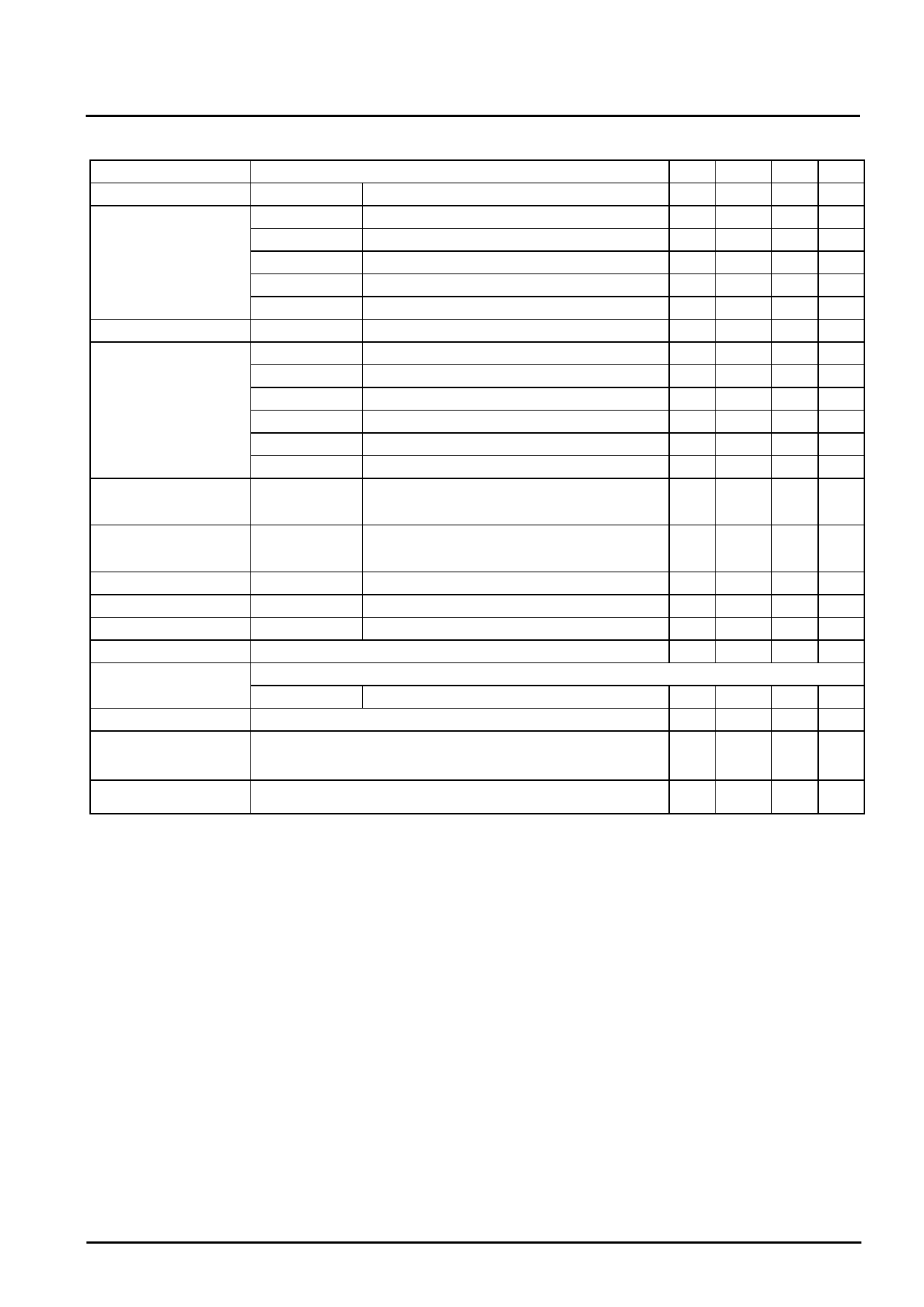
Electrical Characteristics
Parameter
Reference Voltage
GM1117AADJ
GM1117A-1.5
GM1117A-1.8
Output Voltage
GM1117A-2.5
GM1117A-3.3
GM1117A-5.0
Line Regulation
GM1117A-XXX
GM1117AADJ
GM1117A-1.5
Load Regulation
GM1117A-1.8
GM1117A-2.5
GM1117A-3.3
GM1117A-5.0
Conditions
MIN
Io=10mA, Tj=25 , (Vin-Vout )=1.5V
1.225
Io=10mA, Tj=25 , 3.0V Vin 12V
1.470
Io=10mA, Tj=25 , 3.3V Vin 12V
1.764
Io=10mA, Tj=25 , 4.0V Vin 12V
2.450
Io=10mA, Tj=25 , 4.8V Vin 12V
3.235
Io=10mA, Tj=25 , 6.5V Vin 12V
4.900
Io=10mA, Vout+1.5V<Vin<12V, Tj=25
-
Vin=3.3V, Vadj=0, 0mA<Io<1A, Tj=25 (Note 1,2) -
Vin=3.0V, 0mA<Io<1A, TJ=25 (Note 1,2)
-
Vin=3.3V, 0mA<Io<1A, TJ=25 (Note 1,2)
-
Vin=4.0V, 0mA<Io<1A, TJ=25 (Note 1,2)
-
Vin=5.0V, 0mA<Io<1A, TJ=25 (Note 1,2)
-
Vin=8.0V, 0mA<Io<1A, TJ=25 (Note 1,2)
-
TYP
1.250
1.500
1.800
2.500
3.300
5.000
-
-
12
15
20
26
40
MAX UNIT
1.275 V
1.530 V
1.836 V
2.550 V
3.365 V
5.100 V
0.2 %
1%
15 mV
18 mV
25 mV
33 mV
50 mV
Dropout Voltage
(VIN-VOUT)
GM1117A-XXX Io=1A, ( Vout=0.1% Vout)
-
1.3 1.4 V
Current Limit
GM1117A-XXX Vin-Vout=5V
1.1
-
-
A
Minimum Load Current Adjustable model Vin=5V
-
5
10 mA
Adjust Pin Current
Adjustable model Vin=12V, Io=10mA
-
50 100 uA
Quiescent Current
fixed model
Vin=12V, Io=0mA
-
-
12 mA
Thermal Regulation
TA=25 ,30ms pulse
- 0.008 0.04 %/W
Ripple Rejection
F=120HZ,COUT=25uF Tantalum, IOUT=1A
GM1117A-XXX VIN=VOUT+3V
-
60 70 dB
Temperature Stability IO=10mA
-
0.5
-
%
JA Thermal Resistance
Junction-to-Ambient(No
heat sink ;No air flow)
-
300
-
/W
JC Thermal Resistance
Junction-to-Case
Control Circuitry/Power Transistor
-
100
-
/W
Note 1: See thermal regulation specifications for changes in output voltage due to heating effects. Line and load regulation
are measured at a constant junction Temperature by low duty cycle pulse testing. Load regulation is measured at the
output lead =1/18” from the package.
Note 2: Line and load regulation are guaranteed up to the maximum power dissipation of 3W. Power dissipation is
determined by the difference in input and output and the output current. Guaranteed maximum power dissipation will
not be available over the full input/output range.
GM1117A
Page: 3/4
Share Link: 