AMS1501CD 查看數據表(PDF) - Advanced Monolithic Systems Inc
零件编号
产品描述 (功能)
比赛名单
AMS1501CD Datasheet PDF : 9 Pages
| |||
Junction-to-Case
M & D Package: Control Circuitry/ Power Transistor
0.65/2.70
°C/W
AMS1501
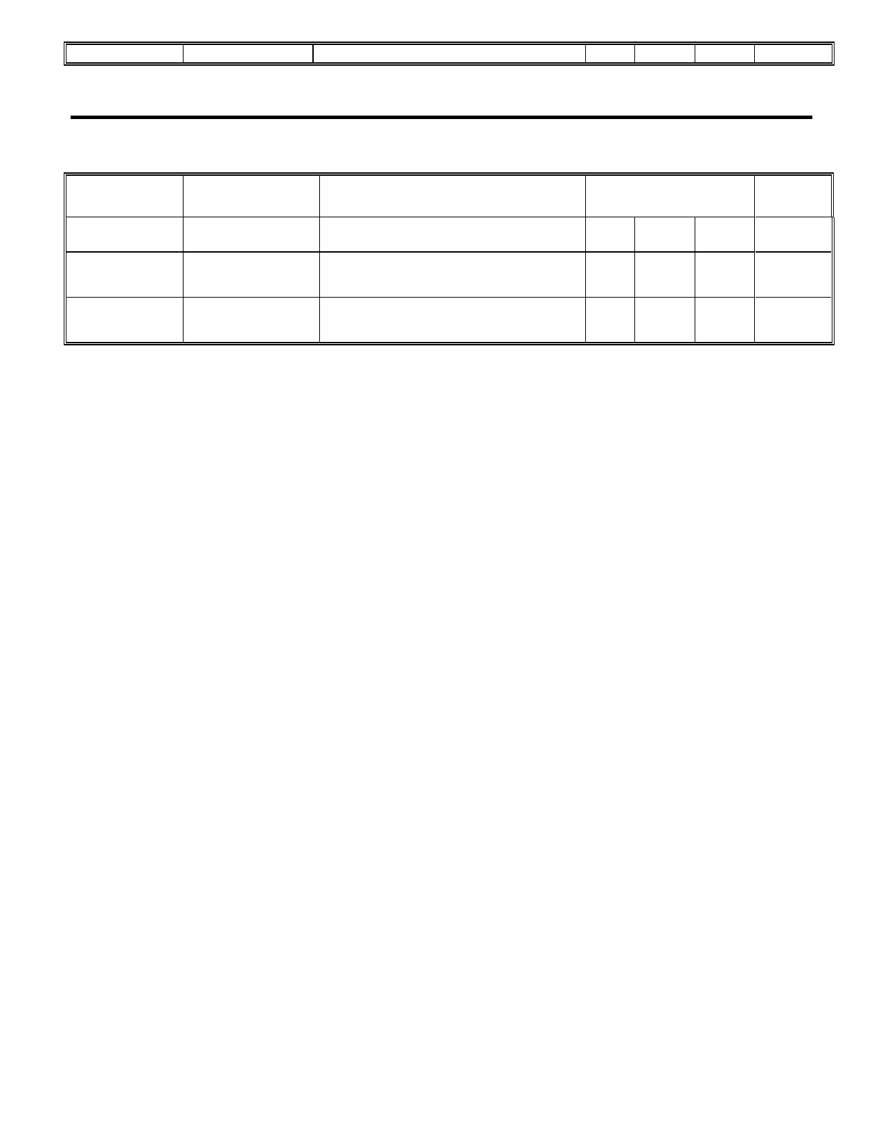
ELECTRICAL CHARACTERISTICS
Electrical Characteristics at IOUT = 0 mA, and TJ = +25°C unless otherwise specified.
Parameter
Device
Conditions
Min Typ Max Units
Dropout Voltage
Note 2
Control Dropout
(VCONTROL - VOUT)
Power Dropout
(VPOWER - VOUT)
AMS1501/-1.5/-2.5/
-2.85/-3.0/-3.3/-3.5/-5.0
AMS1501/-1.5/-2.5/
-2.85/-3.0/-3.3/-3.5/-5.0
VPOWER =VOUT + 0.8V, ILOAD = 10mA
VPOWER =VOUT + 0.8V, ILOAD = 1.5A
VCONTROL =VOUT + 2.5V, ILOAD = 10mA
VCONTROL =VOUT + 2.5V, ILOAD = 1.5A
1.00
1.15
V
1.15
1.30
V
.10
0.17
V
.45
.50
V
Parameters identified with boldface type apply over the full operating temperature range.
Note 1: Absolute Maximum Ratings indicate limits beyond which damage to the device may occur. For guaranteed specifications and test conditions, see the
Electrical Characteristics. The guaranteed specifications apply only for the test conditions listed.
Note 2: Unless otherwise specified VOUT = VSENSE. For the adjustable device VADJ = 0V.
Note 3: The dropout voltage for the AMS1501 is caused by either minimum control voltage or minimum power voltage. The specifications represent the
minimum input/output voltage required to maintain 1% regulation.
Note 4: For the adjustable device the minimum load current is the minimum current required to maintain regulation. Normally the current in the resistor
divider used to set the output voltage is selected to meet the minimum load current requirement.
Note 5: The control pin current is the drive current required for the output transistor. This current will track output current with a ratio of about 1:100. The
minimum value is equal to the quiescent current of the device.
PIN FUNCTIONS
Sense (Pin 1): This pin is the positive side of the reference
voltage for the device. With this pin it is possible to Kelvin
sense the output voltage at the load.
Adjust (Pin 2/5): This pin is the negative side of the
reference voltage for the device. Adding a small bypass
capacitor from the Adjust pin to ground improves the
transient response. For fixed voltage devices the Adjust
pin is also brought out to allow the user to add a bypass
capacitor.
GND (Pin 2/5): For fixed voltage devices this is the
bottom of the resistor divider that sets the output voltage.
VPOWER (Pin 5/6): This pin is the collector to the power
device of the AMS1501. The output load current is
supplied through this pin. The voltage at this pin must
be between 0.1V and 0.8V greater than the output
voltage for the device to regulate.
VCONTROL (Pin 4/3): This pin is the supply pin for the
control circuitry of the device. The current flow into
this pin will be about 1% of the output current. The
voltage at this pin must be 1.3V or greater than the
output voltage for the device to regulate.
Output (Pin 3/4): This is the power output of the
device.
Advanced Monolithic Systems, Inc. www.advanced-monolithic.com Phone (925) 443-0722 Fax (925) 443-0723
Share Link: 