HD74HC367 查看數據表(PDF) - Renesas Electronics
零件编号
产品描述 (功能)
比赛名单
HD74HC367 Datasheet PDF : 7 Pages
| |||
HD74HC367
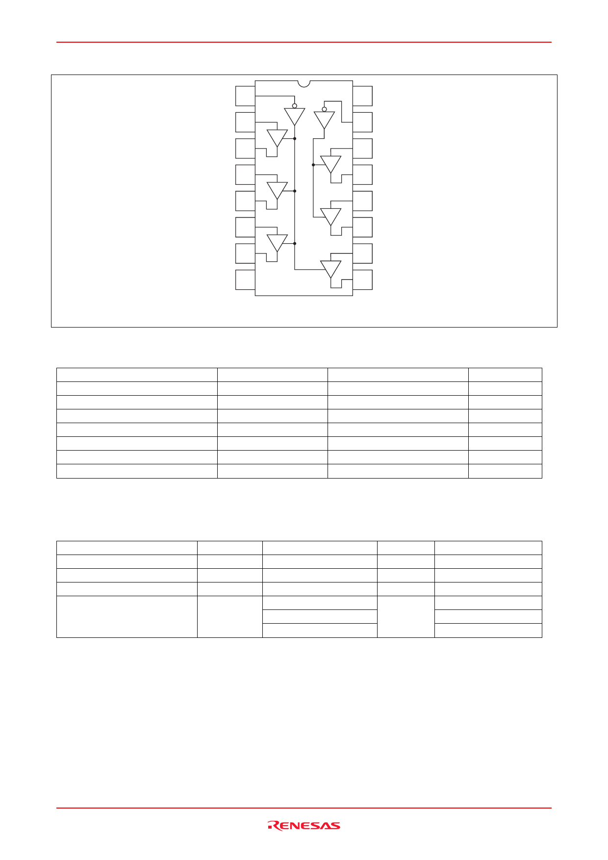
Pin Arrangement
Output
control G1
1
1A 2
1Y 3
2A 4
2Y 5
3A 6
3Y 7
GND 8
(Top view)
16 VCC
15 Output
control G2
14 6A
13 6Y
12 5A
11 5Y
10 4A
9 4Y
Absolute Maximum Ratings
Item
Symbol
Ratings
Unit
Supply voltage range
VCC
–0.5 to 7.0
V
Input / Output voltage
VIN, VOUT
–0.5 to VCC +0.5
V
Input / Output diode current
IIK, IOK
±20
mA
Output current
IOUT
±35
mA
VCC, GND current
ICC or IGND
±75
mA
Power dissipation
PT
500
mW
Storage temperature
Tstg
–65 to +150
°C
Note: The absolute maximum ratings are values, which must not individually be exceeded, and furthermore, no two of
which may be realized at the same time.
Recommended Operating Conditions
Item
Symbol
Ratings
Supply voltage
VCC
2 to 6
Input / Output voltage
VIN, VOUT
0 to VCC
Operating temperature
Input rise / fall time*1
Ta
–40 to 85
tr, tf
0 to 1000
0 to 500
0 to 400
Notes: 1. This item guarantees maximum limit when one input switches.
Waveform: Refer to test circuit of switching characteristics.
Unit
V
V
°C
ns
Conditions
VCC = 2.0 V
VCC = 4.5 V
VCC = 6.0 V
Rev.2.00 Jan 31, 2006 page 2 of 6
Share Link: 