HD74HC373 查看數據表(PDF) - Renesas Electronics
零件编号
产品描述 (功能)
比赛名单
HD74HC373 Datasheet PDF : 10 Pages
| |||
HD74HC373, HD74HC533
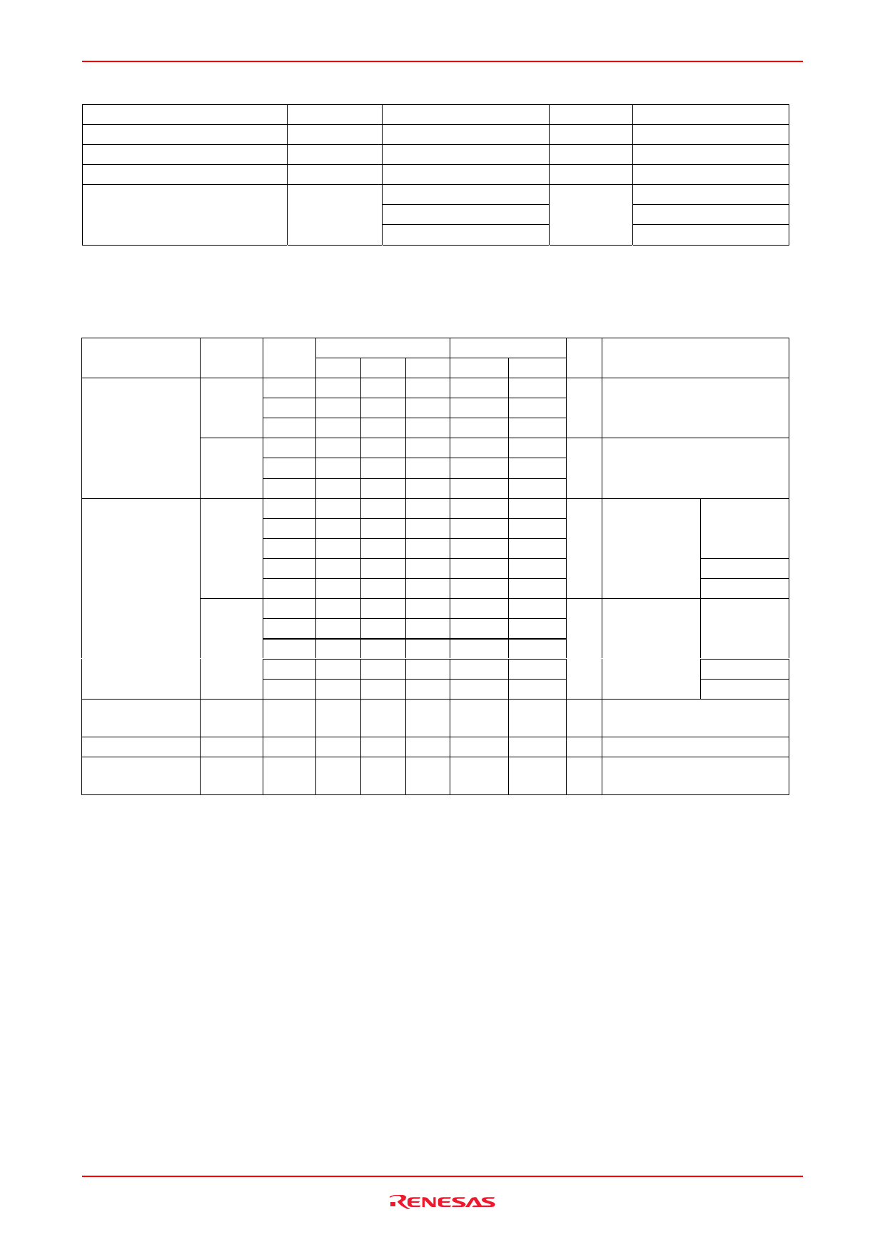
Recommended Operating Conditions
Item
Symbol
Ratings
Supply voltage
Input / Output voltage
VCC
VIN, VOUT
2 to 6
0 to VCC
Operating temperature
Ta
–40 to 85
Input rise / fall time*1
0 to 1000
tr, tf
0 to 500
0 to 400
Note: 1. This item guarantees maximum limit when one input switches.
Waveform: Refer to test circuit of switching characteristics.
Unit
V
V
°C
ns
Conditions
VCC = 2.0 V
VCC = 4.5 V
VCC = 6.0 V
Electrical Characteristics
Item
Input voltage
Output voltage
Off-state output
current
Input current
Quiescent supply
current
Symbol
VIH
VIL
VOH
VOL
IOZ
Iin
ICC
VCC (V)
2.0
4.5
6.0
2.0
4.5
6.0
2.0
4.5
6.0
4.5
6.0
2.0
4.5
6.0
4.5
6.0
6.0
6.0
6.0
Ta = 25°C
Min Typ Max
1.5 — —
3.15 — —
4.2 — —
— — 0.5
— — 1.35
— — 1.8
1.9 2.0 —
4.4 4.5 —
5.9 6.0 —
4.18 — —
5.68 — —
— 0.0 0.1
— 0.0 0.1
— 0.0 0.1
— — 0.26
— — 0.26
— — ±0.5
— — ±0.1
— — 4.0
Ta = –40 to+85°C
Min Max Unit
Test Conditions
1.5
—
V
3.15
—
4.2
—
—
0.5 V
—
1.35
—
1.8
1.9
—
V Vin = VIH or VIL IOH = –20 µA
4.4
—
5.9
—
4.13
—
IOH = –6 mA
5.63
—
IOH = –7.8 mA
—
0.1
V Vin = VIH or VIL IOL = 20 µA
—
0.1
—
0.1
—
0.33
IOH = 6 mA
—
0.33
IOH = 7.8 mA
—
±5.0 µA Vin = VIH or VIL,
Vout = VCC or GND
—
±1.0 µA Vin = VCC or GND
—
40 µA Vin = VCC or GND, Iout = 0 µA
Rev.2.00 Mar 30, 2006 page 4 of 9
Share Link: 