HD74HC374 查看數據表(PDF) - Renesas Electronics
零件编号
产品描述 (功能)
比赛名单
HD74HC374
Renesas Electronics

HD74HC374 Datasheet PDF : 9 Pages
| |||
HD74HC374, HD74HC534
Switching Characteristics (CL = 50 pF, Input tr = tf = 6 ns)
Item
Maximum clock
frequency
Propagation delay
time
Output enable
time
Output disable
time
Setup time
Hold time
Pulse width
Output rise/fall
time
Input capacitance
Symbol VCC (V)
fmax
2.0
4.5
6.0
tPHL
2.0
tPLH
4.5
6.0
tZL
2.0
4.5
6.0
tZH
2.0
4.5
6.0
tLZ
2.0
4.5
6.0
tHZ
2.0
4.5
6.0
tsu
2.0
4.5
6.0
th
2.0
4.5
6.0
tw
2.0
4.5
6.0
tTLH
2.0
tTHL
4.5
6.0
Cin
—
Ta = 25°C
Min Typ Max
—— 6
— — 30
— — 35
— — 140
— 18 28
— — 24
— — 150
— 11 30
— — 26
— — 150
— 14 30
— — 26
— — 150
— 13 30
— — 26
— — 150
— 16 30
— — 26
100 — —
20 1 —
17 — —
25 — —
5
1—
5 ——
80 — —
16 6 —
14 — —
— — 60
— 4 12
— — 10
— 5 10
Ta = –40 to +85°C
Min
Max Unit
Test Conditions
—
5 MHz
—
24
—
28
—
175 ns
—
35
—
30
—
190 ns
—
38
—
33
—
190 ns
—
38
—
33
—
190 ns
—
38
—
33
—
190 ns
—
38
—
33
125
—
ns Data to Clock
25
—
21
—
31
—
ns Clock to Data
6
—
6
—
100
—
ns Clock or Output control
20
—
17
—
—
75
ns
—
15
—
13
—
10
pF
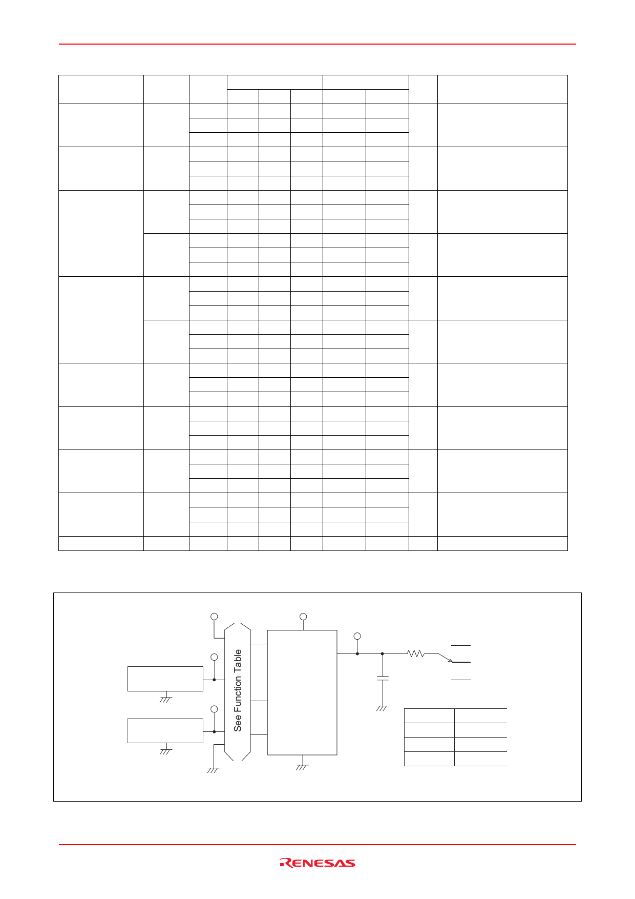
Test Circuit
VCC
Input
Pulse Generator
Zout = 50 Ω
Input
Pulse Generator
Zout = 50 Ω
VCC
Output
OC 1Q to 8Q
or
1Q to 8Q
1D to 8D
Clock
1 k Ω S1
CL =
50 pF
OPEN
GND
VCC
TEST
tPLH / t PHL
tZH/ t HZ
tZL / t LZ
S1
OPEN
GND
VCC
Note : 1. CL includes probe and jig capacitance.
Rev.2.00 Mar 30, 2006 page 5 of 8
Share Link: