HD74LS166A 查看數據表(PDF) - Renesas Electronics
零件编号
产品描述 (功能)
比赛名单
HD74LS166A Datasheet PDF : 8 Pages
| |||
HD74LS166A
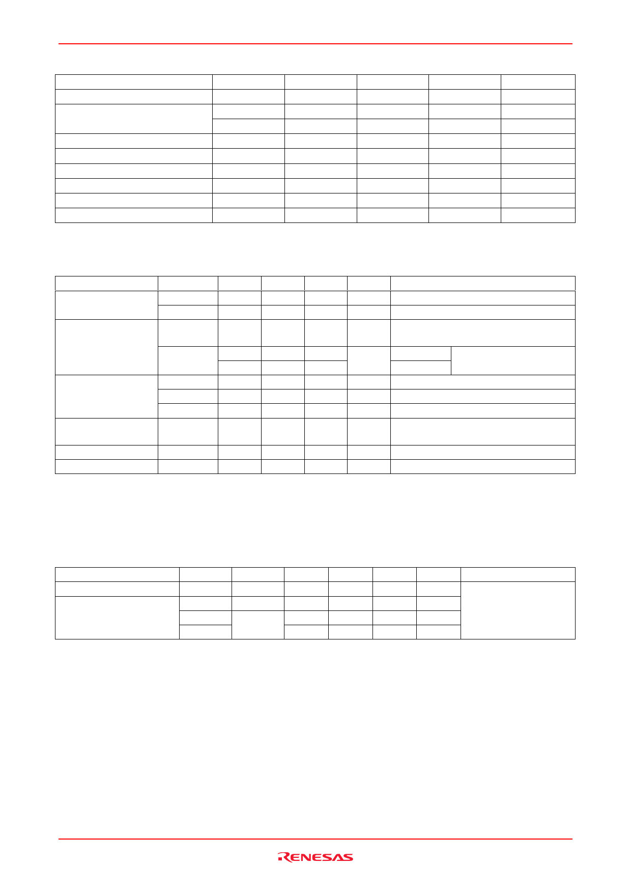
Recommended Operating Conditions
Item
Supply voltage
Output current
Operating temperature
Clock frequency
Clock and clear pulse width
Mode control setup time
Data setup time
Hold time
Symbol
VCC
IOH
IOL
Topr
ƒclock
tw
tsu
tsu
th
Min
4.75
—
—
–20
0
20
30
20
0
Typ
Max
Unit
5.00
5.25
V
—
–400
µA
—
8
mA
25
75
°C
—
25
MHz
—
—
ns
—
—
ns
—
—
ns
—
—
ns
Electrical Characteristics
(Ta = –20 to +75 °C)
Item
Symbol
min.
typ.* max.
Unit
Condition
Input voltage
Output voltage
Input current
Short-circuit output
current
VIH
2.0
—
—
V
VIL
—
—
0.8
V
VOH
2.7
—
—
V
VCC = 4.75 V, VIH = 2 V, VIL = 0.8 V,
IOH = –400 µA
VOL
—
—
0.4
V
IOL = 4 mA VCC = 4.75 V, VIH = 2 V,
—
—
0.5
IOL = 8 mA VIL = 0.8 V
IIH
—
—
20
µA VCC = 5.25 V, VI = 2.7 V
IIL
—
—
–0.4
mA VCC = 5.25 V, VI = 0.4 V
II
—
—
0.1
mA VCC = 5.25 V, VI = 7 V
IOS
–20
—
–100
mA VCC = 5.25 V
Supply current**
ICC
—
20
32
mA VCC = 5.25 V
Input clamp voltage
VIK
—
—
–1.5
V
VCC = 4.75 V, IIN = –18 mA
Notes: * VCC = 5 V, Ta = 25°C
** With the outputs open, 4.5 V applied to the serial input and all other inputs except the clock grounded, ICC is
measured after a momentary ground, then 4.5 V, is applied to clock.
Switching Characteristics
(VCC = 5 V, Ta = 25°C)
Item
Symbol Inputs min.
typ.
max.
Unit
Condition
Maximum clock frequency
ƒmax
25
35
—
MHz
Propagation delay time
tPHL
tPHL
Clear
—
7
Clock
19
14
30
25
ns
ns
CL = 15 pF, RL = 2 kΩ
tPLH
5
11
20
ns
Rev.4.00, May 10, 2006, page 4 of 7
Share Link: 