HD74LVC1G66CPE 查看數據表(PDF) - Renesas Electronics
零件编号
产品描述 (功能)
比赛名单
HD74LVC1G66CPE Datasheet PDF : 10 Pages
| |||
HD74LVC1G66
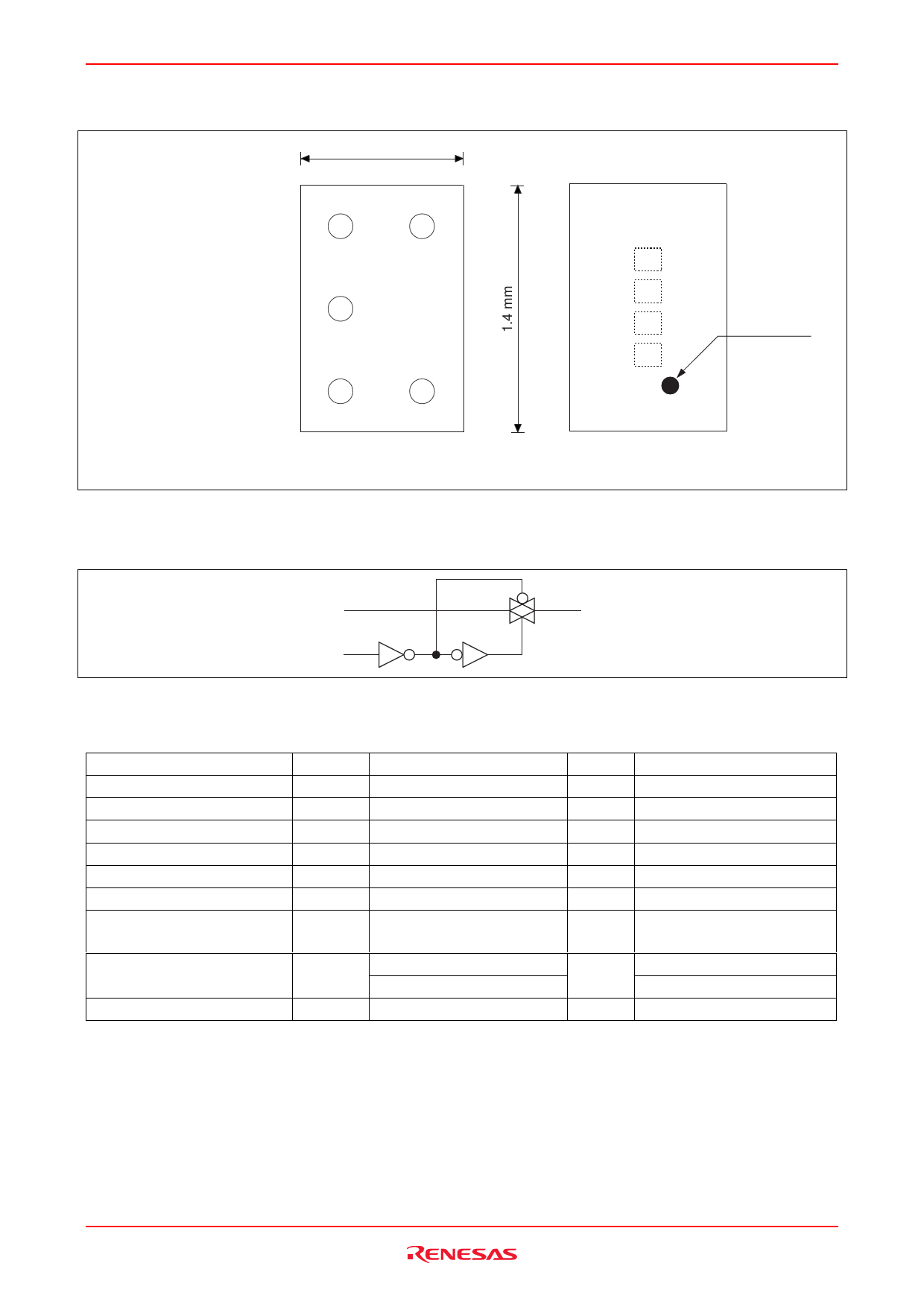
Pin Arrangement
Height 0.5 mm
0.5 mm pitch
0.17 mm 5–Ball (CP)
0.23 mm 5–Ball (CL)
GND
OUT/IN
0.9 mm
34
2
CONT
IN/OUT
15
VCC
Pin#1 INDEX
Logic Diagram
(Bottom view)
IN/OUT 1
4
CONT
(Top view)
2 OUT/IN
Absolute Maximum Ratings
Item
Symbol
Ratings
Unit
Test Conditions
Supply voltage range
VCC
–0.5 to 6.5
Input voltage range *1
VI
–0.5 to 6.5
Output voltage range *1, 2
VO
–0.5 to VCC +0.5
V
V
V
Output : H or L
Control Input clamp current
IIK
–50
Output clamp current
IOK
±50
mA
VI < 0
mA
VO < 0 or VO > VCC
Continuous output current
IO
±50
mA
VO = 0 to VCC
Continuous current through
VCC or GND
Package Thermal impedance
ICC or IGND ±100
θja
154
mA
°C/W CP
132
CL
Storage temperature
Tstg
–65 to 150
°C
Notes:
The absolute maximum ratings are values, which must not individually be exceeded, and furthermore no two
of which may be realized at the same time.
1. The input and output voltage ratings may be exceeded if the input and output clamp-current ratings are
observed.
2. This value is limited to 5.5 V maximum.
Rev.3.00 Jul. 01, 2004 page 2 of 10
Share Link: 