HD74LVC1G97 查看數據表(PDF) - Renesas Electronics
零件编号
产品描述 (功能)
比赛名单
HD74LVC1G97 Datasheet PDF : 11 Pages
| |||
HD74LVC1G97
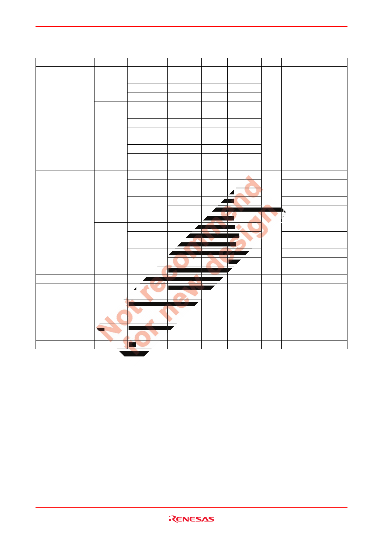
Electrical Characteristics
Ta = –40 to 85°C
Item
Threshold voltage
Symbol
VT+
VCC (V)
1.8
2.5
Min
0.8
1.2
Typ
—
—
Max
1.4
1.7
Unit
V
Test condition
3.3
1.6
—
2.3
5.0
VT–
1.8
2.5
2.3
—
3.0
0.4
—
0.7
0.6
—
1.0
3.3
0.9
—
1.4
5.0
1.5
—
2.0
∆VT
1.8
2.5
0.4
—
0.7
0.4
—
0.8
3.3
0.4
—
0.9
5.0
0.4
—
1.0
Output voltage
VOH
VOL
Input current
IIN
Quiescent
ICC
supply current
∆ICC
1.65 to 5.5 VCC–0.1 —
—
1.65
1.2
—
—
2.3
1.9
—
—
3.0
2.4
—
—
2.3
—
—
4.5
3.8
—
—
1.65 to 5.5 —
—
0.1
1.65
—
—
0.45
2.3
—
—
0.3
3.0
—
—
0.4
0.55
4.5
—
—
0.55
0 to 5.5
—
—
±5
5.5
—
—
10
3 to 5.5
—
—
500
V
IOH = 100 µA
IOH = –4 mA
IOH = –8 mA
IOH = –16 mA
IOH = –24 mA
IOH = –32 mA
IOL = 100 µA
IOL = 4 mA
IOL = 8 mA
IOL = 16 mA
IOL = 24 mA
IOL = 32 mA
µA VIN = 5.5 V or GND
µA VIN = VCC or GND,
IO = 0
One input at VCC–0.6 V,
Other input at VCC or
GND
Output leakage
IOFF
0
current
—
—
±10
µA VIN or VO = 0 to 5.5 V
Input capacitance CIN
3.3
—
3.5
—
pF
VIN = VCC or GND
Note: For conditions shown as Min or Max, use the appropriate values under recommended operating conditions.
Rev.4.00 Jun. 29, 2004 page 6 of 10
Share Link: 