HD74LVC2G66 查看數據表(PDF) - Renesas Electronics
零件编号
产品描述 (功能)
比赛名单
HD74LVC2G66 Datasheet PDF : 12 Pages
| |||
HD74LVC2G66
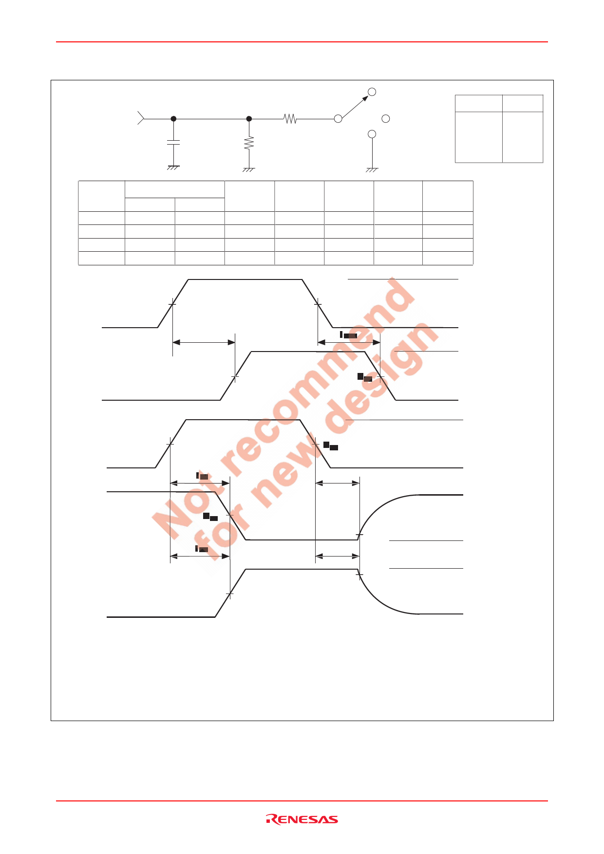
Test Circuit (cont.)
From Output
CL
Load circuit
RL
S1
VTT
OPEN
GND
RL
TEST
S1
tPLH / tPHL
tZH / tHZ
tZL / tLZ
OPEN
GND
VTT
VCC (V)
1.8±0.15
2.5±0.2
3.3±0.3
5.0±0.5
INPUTS
VI
VCC
VCC
VCC
VCC
tr / tf
≤ 2 ns
≤ 2 ns
≤ 2.5 ns
≤ 2.5 ns
Vref
VCC / 2
VCC / 2
VCC / 2
VCC / 2
VTT
2 × VCC
2 × VCC
2 × VCC
2 × VCC
CL
30 pF
30 pF
50 pF
50 pF
RL
1.0 kΩ
500 Ω
500 Ω
500 Ω
∆V
0.15 V
0.15 V
0.3 V
0.3 V
VI
Input
Vref
Vref
Output
t PLH
Vref
t PHL
Vref
0V
V OH
V OL
VI
Control
Vref
Vref
Input
t ZL
t LZ
0V
VOH
Output
(Waveform – A)
Vref
t ZH
VOL + ∆V
t HZ
V OL
Output
(Waveform – B)
Vref
VOH – ∆V
V OH
VOL
Notes: 1. CL includes probe and jig capacitance.
2. Waveform–A is for an output with internal conditions such that the output is low except
when disabled by the output control.
3. Waveform–B is for an output with internal conditions such that the output is high except
when disabled by the output control.
4. All input pulses are supplied by generators having the following characteristics:
PRR ≤ 10MHz, Zo = 50 Ω.
5. The output are measured one at a time with one transition per measurement.
Rev.3.00 Jul 07, 2005 page 8 of 11
Share Link: 