HMP8115CN 查看數據表(PDF) - Intersil
零件编号
产品描述 (功能)
比赛名单
HMP8115CN Datasheet PDF : 43 Pages
| |||
HMP8115
BUILT-IN VIDEO GENERATION
When the blue screen, black screen or color bar output is
selected, a full-screen of blue, black or 75% colorbar output
is generated using the currently selected output format. The
type of screen to be generated is determined by bits 2 and 1
of the OUTPUT FORMAT register 02H. When built-in video
generation is not desired, the bits need to be set for normal
operation to pass decoded video.
If a video source is input, it will be used to provide the video
timing. If an input video source is not detected, internally-
generated video timing will be used.
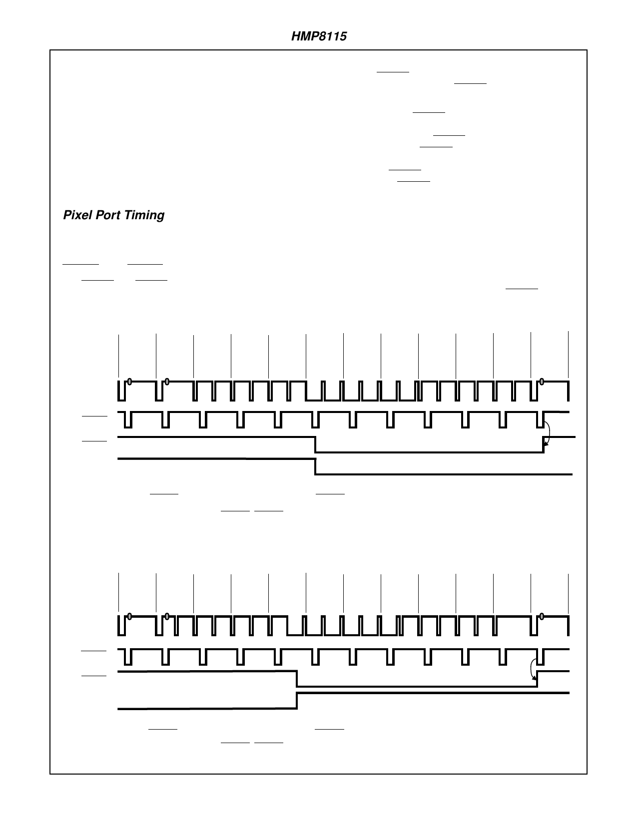
Pixel Port Timing
The the timing and format of the output data and control sig-
nals is presented in the following sections.
HSYNC AND VSYNC TIMING
The HSYNC and VSYNC output timing is VMI v1.4 compati-
ble. Figures 5-8 illustrate the video timing. The leading edge
of HSYNC is synchronous to the video input signal and has
a fixed latency due to internal pipeline processing. The pulse
width of the HSYNC is defined by the END HSYNC register
36H, where the trailing edge of HSYNC has a programmable
delay of 0-510 CLK2 cycles from the leading edge.
The leading edge of VSYNC is asserted approximately half
way through the first serration pulse of each field. For an odd
field, the trailing edge of VSYNC is 5±1 CLK2 cycles after
the trailing edge of the HSYNC that follows the last equaliza-
tion pulse. Refer to Figures 5 and 7. For an even field, the
trailing edge of VSYNC is 5±1 CLK2 cycles leading the lead-
ing edge of the HSYNC that follows the last equalization
pulse. Refer to Figures 6 and 8.
FIELD TIMING
When field information can be determined from the input
video source, the FIELD output pin reflects the video source
field state. When field information cannot be determined
from the input video source, the FIELD output pin alternates
its state at the beginning of each field. FIELD changes state
5±1 CLK2 cycles before the leading edge of VSYNC.
NTSC(M)
LINE #
524
525
1
2
3
4
5
6
7
8
9
10
PAL(M)
521
522
523
524
525
1
2
3
4
5
6
7
LINE #
VIDEO
INPUT
HSYNC
VSYNC
FIELD
‘EVEN’ FIELD
‘ODD’ FIELD
NOTE:
3. The trailing edge of VSYNC is 5±1 clocks after the trailing edge of HSYNC to be VMI compatible and to indicate a transition to an odd field.
FIGURE 5. NTSC(M) AND PAL(M) HSYNC, VSYNC AND FIELD TIMING DURING AN EVEN TO ODD FIELD TRANSITION
NTSC(M)
LINE #
262
263
264
265
266
267
268
269
270
271
272
273
PAL(M)
259
260
261
262
263
264
265
266
267
268
269
270
LINE #
VIDEO
INPUT
HSYNC
VSYNC
FIELD
‘ODD’ FIELD
‘EVEN’ FIELD
NOTE:
4. The trailing edge of VSYNC is 5±1 clocks after the leading edge of HSYNC to be VMI compatible and to indicate a transition to an even field.
FIGURE 6. NTSC(M) AND PAL(M) HSYNC, VSYNC AND FIELD TIMING DURING AN ODD TO EVEN FIELD TRANSITION
9
Share Link: 