HT7718(2007) 查看數據表(PDF) - Holtek Semiconductor
零件编号
产品描述 (功能)
比赛名单
HT7718 Datasheet PDF : 19 Pages
| |||
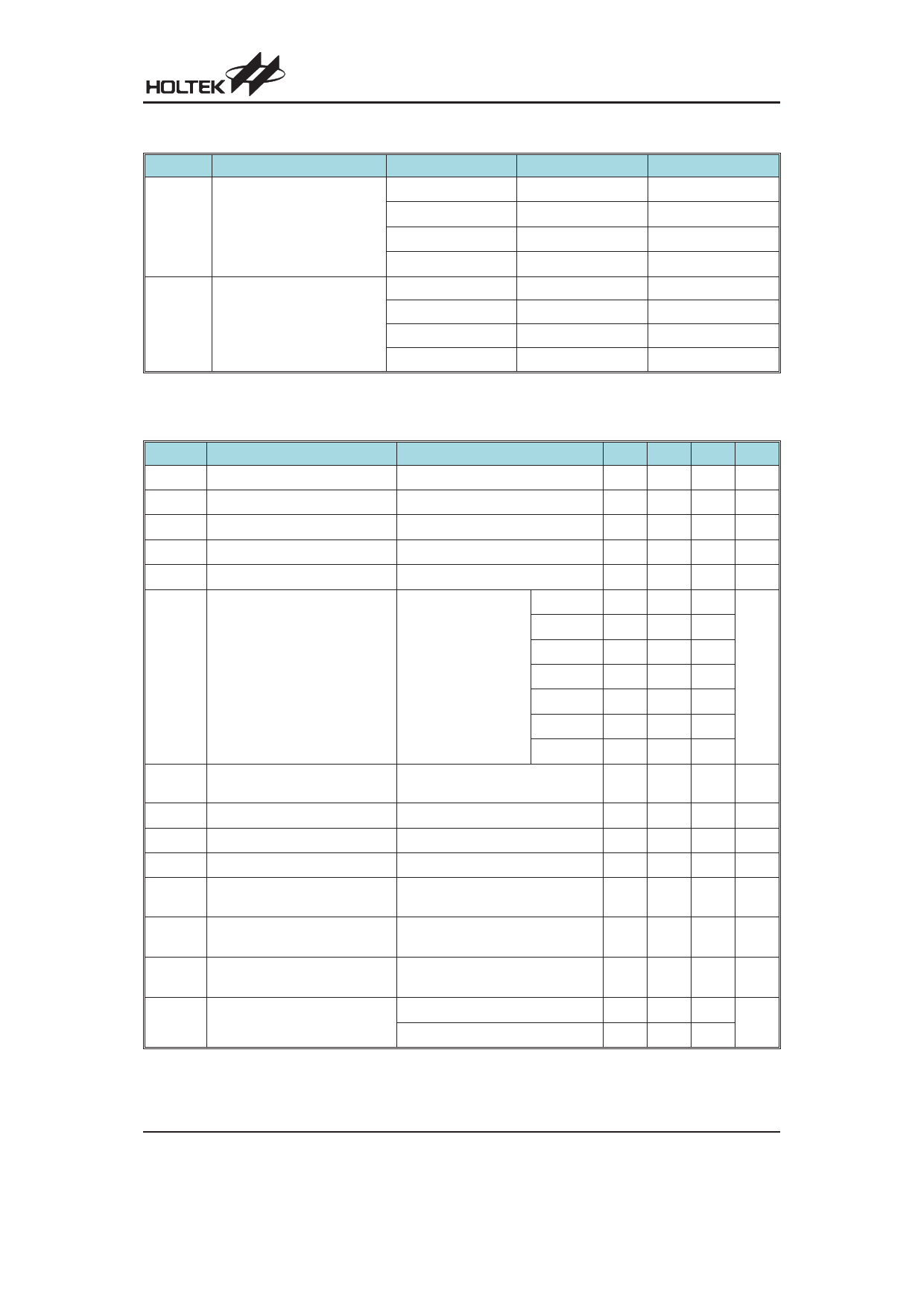
HT77XX
Electrical Characteristics
VIN=VOUT´0.6; IOUT=10mA; Ta=25°C (Unless otherwise specified)
Symbol
Parameter
Test Conditions
Min.
VIN
Input Voltage
¾
¾
DVOUT
VSTART
VHOLD
IIN
Output Voltage Tolerance
¾
-2.5
Start-up Voltage (Fig. 1)
VIN: 0®2V; IOUT=1mA
¾
Minimum Hold-on Voltage (Fig. 1) VIN: 2®0V; IOUT=1mA
¾
No-load Input Current (Fig. 1) IOUT=0mA
¾
VOUT=1.8V ¾
VOUT=2.7V ¾
IDD1
Supply Current 1 (Fig. 2)
VS=VOUT´0.95
VOUT=3.0V ¾
Measured at VOUT pin VOUT=3.3V ¾
VOUT=3.7V ¾
VOUT=5.0V ¾
IDD2
Supply Current 2 (Fig. 2)
VS=VOUT+0.5V
Measured at VOUT pin
¾
ISHDN
Shutdown Current
CE=GND
¾
VIH
CE High Threshold
¾
2
VIL
CE Low Threshold
¾
¾
ILEAK
LX Leakage Current (Fig. 3)
VS=VOUT+0.5V, VX=6V
Measured at the LX pin
¾
fOSC
Maximum Oscillator Frequency VS=VOUT´0.95
(Fig. 3)
Measured at LX pin
¾
DOSC
Oscillator Duty Cycle (Fig. 3)
VS=VOUT´0.95
Measured at LX pin
65
VOUT£1.8V
¾
h
Efficiency
VOUT³2.7V
¾
Typ.
¾
¾
0.7
¾
10
35
40
45
55
64
85
4
0.5
¾
¾
¾
115
75
80
85
Max.
6
2.5
0.9
0.7
20
50
60
68
81
85
134
7
1
¾
0.4
0.9
¾
85
¾
¾
Unit
V
%
V
V
mA
mA
mA
mA
V
V
mA
kHz
%
%
Note: Absolute maximum ratings indicate limits beyond which damage to the device may occur. Operating Ratings
indicate conditions for which the device is intended to be functional, but do not guarantee specific performance
limits. The guaranteed specifications apply only for the test conditions listed.
Test Circuit
100mH
1N 5817
V IN
V OUT
47mF
LX
( T a n ta lu m )
VO UT
H T77X X
S e r ie s
GND
(F ig . 1 )
100mF
VS
( T a n ta lu m )
VO UT
LX
VS
H T77X X
S e r ie s
GND
VO UT
LX
H T77X X
S e r ie s
100W
GND
VX
(F ig . 2 )
(F ig . 3 )
Rev 1.60
3
September 12, 2007
Share Link: 