HT7750 查看數據表(PDF) - Holtek Semiconductor
零件编号
产品描述 (功能)
比赛名单
HT7750 Datasheet PDF : 19 Pages
| |||
HT77XX
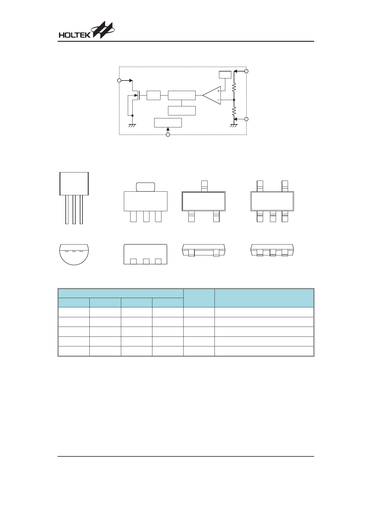
Block Diagram
LX
B u ffe r
P F M C o n tro l
O S C 115kH z
C h ip E n a b le
VO UT
V re f
GND
Pin Assignment
TO 92
123
F r o n t V ie w
G N D V O U T LX
CE
S O T89
1
2
3
G N D V O U T LX
S O T23
VO UT
3
S O T 2 3 -5
LX
GND
5
4
T o p V ie w
T o p V ie w
1
2
GND
LX
1
2
3
CE VO UT NC
B o tto m V ie w
G N D V O U T LX
GND
LX
CE VO UT NC
Pin Description
TO92
Pin No.
SOT89
SOT23
¾
¾
¾
2
2
3
¾
¾
¾
1
1
1
3
3
2
SOT23-5
1
2
3
4
5
Pin Name
Description
CE
VOUT
NC
GND
LX
Chip enable pin, high active
DC/DC converter output monitoring pin
No connection
Ground pin
Switching pin
Absolute Maximum Ratings
Supply Voltage ..............................VSS-0.3V to VSS+7V
Operating Temperature ...........................-40°C to 85°C
Storage Temperature ............................-50°C to 125°C
Note: These are stress ratings only. Stresses exceeding the range specified under ²Absolute Maximum Ratings² may
cause substantial damage to the device. Functional operation of this device at other conditions beyond those listed
in the specification is not implied and prolonged exposure to extreme conditions may affect device reliability.
Rev 1.90
2
October 13, 2010
Share Link: 