ICS671-06 查看數據表(PDF) - Integrated Circuit Systems
零件编号
产品描述 (功能)
比赛名单
ICS671-06 Datasheet PDF : 6 Pages
| |||
ICS671-06
3.3 VOLT ZERO DELAY, LOW SKEW BUFFER
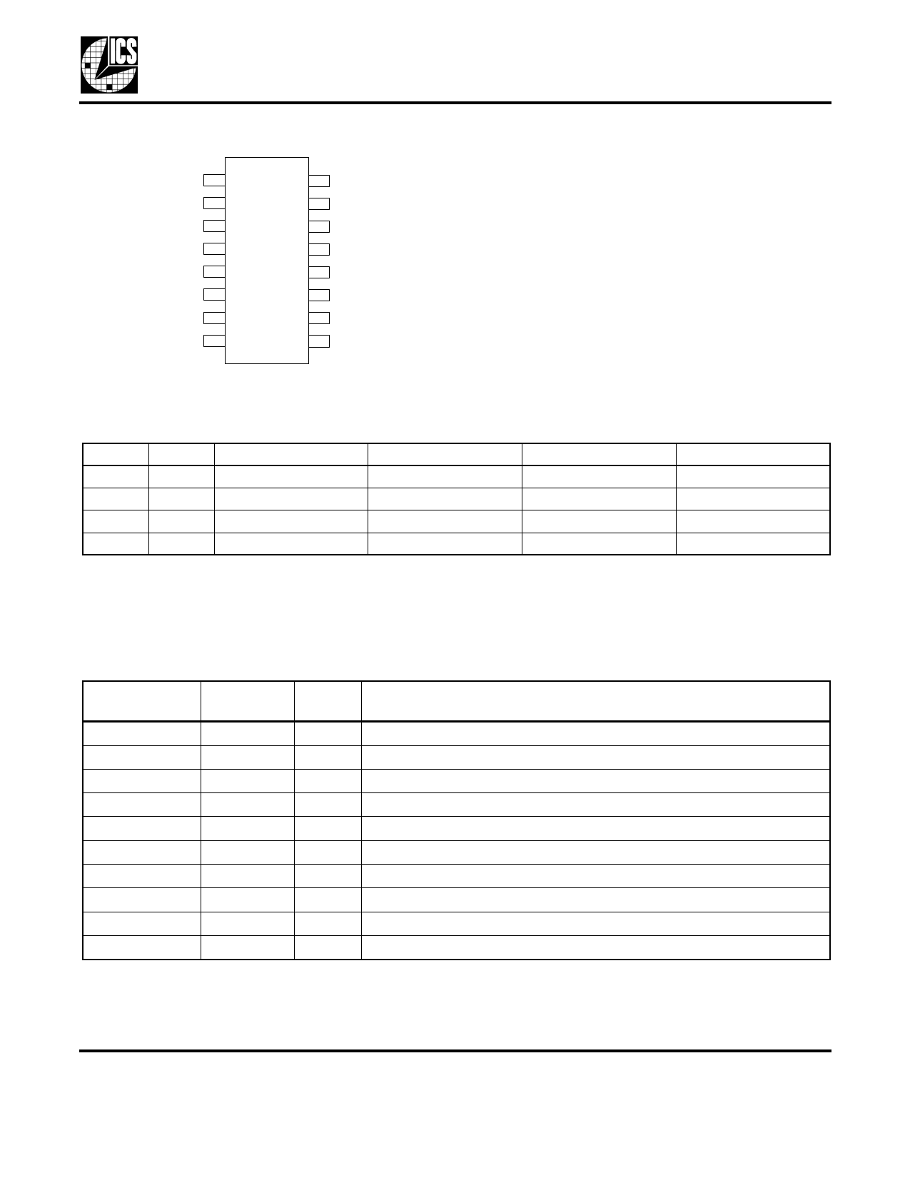
Pin Assignment
C L K IN
1
CLKA1
2
CLKA2
3
VDD
4
GND
5
CLKB1
6
CLKB2
7
S2
8
16
F B IN
15
CLKA4
14
CLKA3
13
VDD
12
GND
11
CLKB4
10
CLKB3
9
S1
16 pin narrow (150 m il) SO IC
and 16pin (173m il ) TSSO P
Output Clock Mode Select Table
S2
S1
0
0
0
1
1
0
1
1
CLKA1:A4
Tri-state (note 1)
Running
Running
Running
CLKB1:B4
Tri-state (note 1)
Tri-state (note 1)
Running
Running
Note 1. Outputs are in high impedance state.
Note 2. Buffer mode only; not zero delay between input and output.
A & B Source
PLL
PLL
CLKIN (note 2)
PLL
PLL Status
OFF
ON
OFF
ON
Pin Descriptions
Pin
Number
1
2 - 3, 14 - 15
4
5
6 - 7, 10 - 11
8
9
12
13
16
Pin
Name
CLKIN
CLKA1:A4
VDD
GND
CLKB1:B4
S2
S1
GND
VDD
FBIN
Pin Type
Pin Description
Input
Output
Power
Power
Output
Input
Input
Power
Power
Input
Clock input.
Clock outputs A1:A4. See table above.
Power supply. Connect to 3.3 V.
Connect to ground.
Clock outputs B1:B4. See table above.
Select input 2. See table above. Internal pull-up.
Select input 1. See table above. Internal pull-up.
Connect to ground.
Power supply. Connect to 3.3 V.
Feedback input. Connect to any output under normal operation.
MDS 671-06 D
2
Revision 050405
Integrated Circuit Systems l 525 Race Street, San Jose, CA 95126 l tel (408) 297-1201 l www.icst.com
Share Link: 