ICS93705 查看數據表(PDF) - Integrated Circuit Systems
零件编号
产品描述 (功能)
比赛名单
ICS93705 Datasheet PDF : 7 Pages
| |||
ICS9370 5
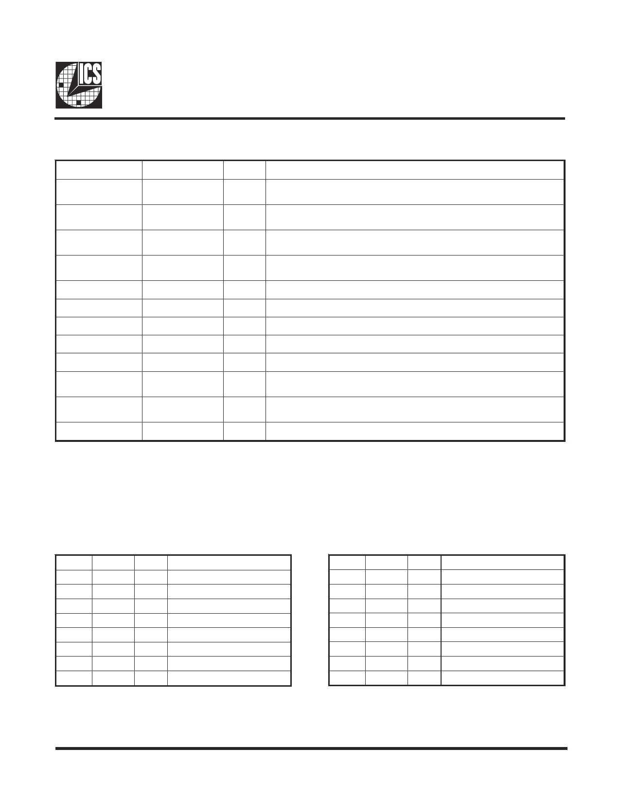
Pin Descriptions
PIN NUMBER
PIN NAME
1, 7, 8, 18, 24, 25,
31, 41, 42, 48
GND
26, 30, 40, 43, 47,
23, 19, 9, 6, 2
CLKC(9:0)
27, 29, 39, 44, 46,
22, 20, 10, 5, 3
CLKT(9:0)
4, 11, 15, 21, 28,
34, 38, 45,
VDD
12
SCLK
13
CLK_INT
14, 32, 36
N/C
16
AVDD
17
AGND
33
FB_OUTT
35
FB_INT
37
SDATA
TYPE
PWR Ground
DESCRIPTION
OUT "Complementary" clocks of differential pair outputs.
OUT "True" Clock of differential pair outputs.
PWR Power supply 2.5V
IN Clock input of I2C input, 5V tolerant input
IN "True" reference clock input, 3.3V tolerant input
- Not connected
PWR Analog power supply, 2.5V
PWR
OUT
IN
I/O
Analog ground.
"True" Feedback output, dedicated for external feedback. It switches at
the same frequency as the CLK. This output must be wired to FB_INT.
"True" Feedback input, provides feedback signal to the internal PLL for
synchronization with CLK_INT to eliminate phase error.
Data pin for I2C circuitry 5V tolerant
Byte 0: Output Control
(1= enable, 0 = disable)
BIT
Bit 7
Bit 6
Bit 5
Bit 4
Bit 3
Bit 2
Bit 1
Bit 0
PIN#
-
-
-
-
-
-
-
-
PWD
DESCRIPTION
1 Reserved
1 Reserved
1 Reserved
1 Reserved
1 Reserved
1 Reserved
1 Reserved
1 Reserved
Byte 1: Output Control
(1= enable, 0 = disable)
BIT
Bit 7
Bit 6
Bit 5
Bit 4
Bit 3
Bit 2
Bit 1
Bit 0
PIN#
-
-
-
-
-
-
-
-
PWD
DESCRIPTION
1 Reserved
1 Reserved
1 Reserved
1 Reserved
1 Reserved
1 Reserved
1 Reserved
1 Reserved
0418C—08/08 /02
2
Share Link: 