IDT2305A 查看數據表(PDF) - Integrated Device Technology
零件编号
产品描述 (功能)
比赛名单
IDT2305A Datasheet PDF : 7 Pages
| |||
IDT2305A
3.3V ZERO DELAY CLOCK BUFFER
COMMERCIAL AND INDUSTRIAL TEMPERATURE RANGES
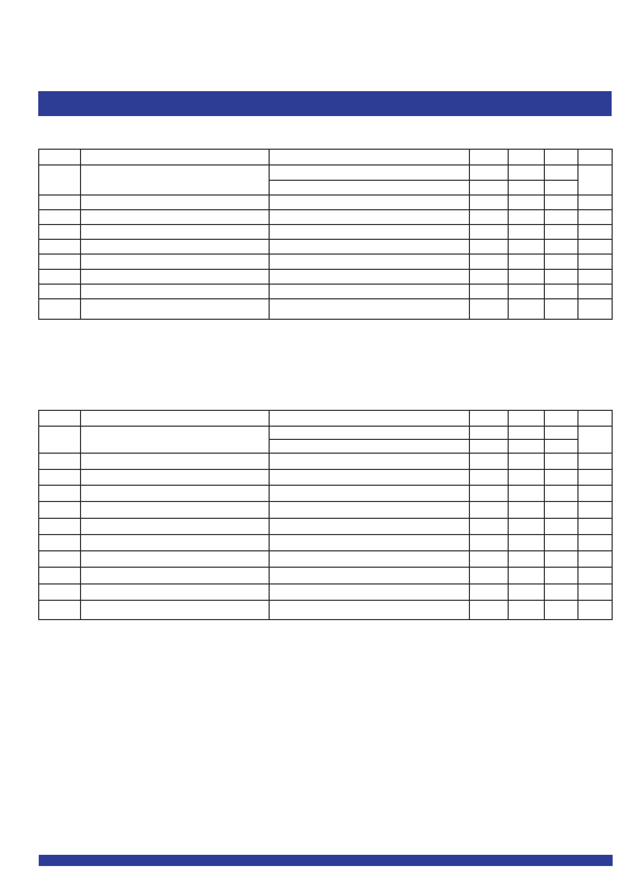
SWITCHING CHARACTERISTICS (2305A-1) - INDUSTRIAL(1,2)
Symbol
Parameter
Conditions
Min.
t1
Output Frequency
10pF Load
10
30pF Load
10
Duty Cycle = t2 ÷ t1
Measured at 1.4V, FOUT = 66.66MHz
40
t3
Rise Time
Measured between 0.8V and 2V
—
t4
Fall Time
Measured between 0.8V and 2V
—
t5
Output to Output Skew
All outputs equally loaded
—
t6
Delay, REF Rising Edge to CLKOUT Rising Edge Measured at VDD/2
—
t7
Device-to-Device Skew
Measured at VDD/2 on the CLKOUT pins of devices
—
tJ
Cycle-to-Cycle Jitter, pk - pk
Measured at 66.66MHz, loaded outputs
—
tLOCK PLL Lock Time
Stable power supply, valid clock presented on REF pin —
Typ. Max. Unit
— 133 MHz
— 100
50 60
%
— 2.5
ns
— 2.5
ns
— 250
ps
0 ±350 ps
0 700
ps
— 200
ps
—
1
ms
NOTES:
1. REF Input has a threshold voltage of VDD/2.
2. All parameters specified with loaded outputs.
SWITCHING CHARACTERISTICS (2305A-1H) - INDUSTRIAL(1,2)
Symbol
Parameter
Conditions
Min.
t1
Output Frequency
10pF Load
10
30pF Load
10
Duty Cycle = t2 ÷ t1
Measured at 1.4V, FOUT = 66.66MHz
40
Duty Cycle = t2 ÷ t1
Measured at 1.4V, FOUT <50MHz
45
t3
Rise Time
Measured between 0.8V and 2V
—
t4
Fall Time
Measured between 0.8V and 2V
—
t5
Output to Output Skew
All outputs equally loaded
—
t6
Delay, REF Rising Edge to CLKOUT Rising Edge Measured at VDD/2
—
t7
Device-to-Device Skew
Measured at VDD/2 on the CLKOUT pins of devices
—
t8
Output Slew Rate
Measured between 0.8V and 2V using Test Circuit #2
1
tJ
Cycle-to-Cycle Jitter, pk - pk
Measured at 66.66MHz, loaded outputs
—
tLOCK PLL Lock Time
Stable power supply, valid clock presented on REF pin —
NOTES:
1. REF Input has a threshold voltage of VDD/2.
2. All parameters specified with loaded outputs.
Typ. Max. Unit
— 133 MHz
— 100
50 60
%
50 55
%
— 1.5
ns
— 1.5
ns
— 250
ps
0 ±350 ps
0 700
ps
— — V/ns
— 200
ps
—
1
ms
ZERO DELAY AND SKEW CONTROL
All outputs should be uniformly loaded in order to achieve Zero I/O Delay. Since the CLKOUT pin is the internal feedback for the PLL, its relative
loading can affect and adjust the input/output delay.
For designs utilizing zero I/O Delay, all outputs including CLKOUT must be equally loaded. Even if the output is not used, it must have a capacitive
load equal to that on the other outputs in order to obtain true zero I/O Delay. If I/O Delay adjustments are needed, use the Output Load Difference diagram
to calculate loading differences between the CLKOUT pin and other outputs. For zero output-to-output skew, all outputs must be loaded equally.
5
Share Link: 