IDT7008S 查看數據表(PDF) - Integrated Device Technology
零件编号
产品描述 (功能)
比赛名单
IDT7008S Datasheet PDF : 19 Pages
| |||
IDT7008S/L
High-Speed 64K x 8 Dual-Port Static RAM
Military, Industrial and Commercial Temperature Ranges
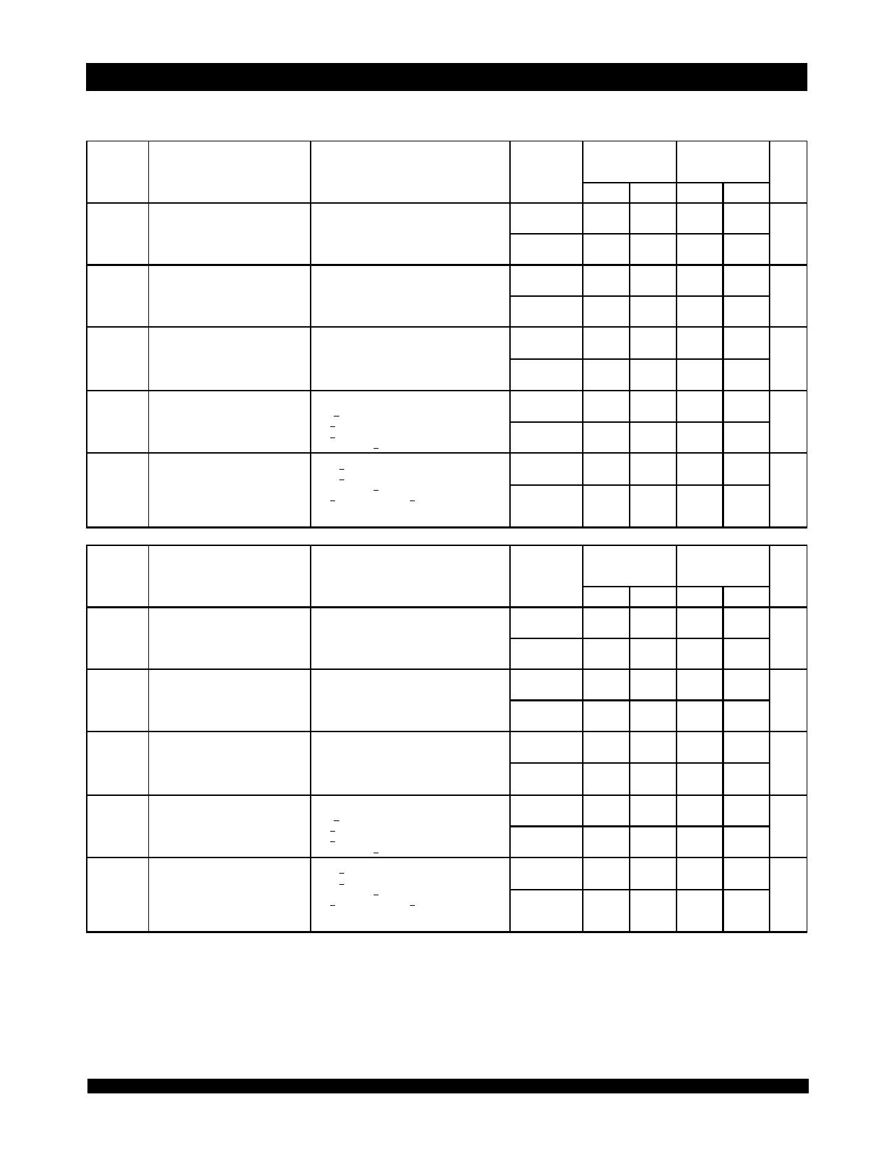
DC Electrical Characteristics Over the Operating
Temperature and Supply Voltage Range(1,6,7) (VCC = 5.0V ± 10%)
7008X20
Com'l Only
Symbol
ICC
Parameter
Dynamic Operating
Current
(Both Ports Active)
IS B1
Standby Current
(Both Ports - TTL Level
Inputs)
IS B2
Standby Current
(One Port - TTL Level
Inputs)
IS B3
Full Standby Current
(Both Ports - All CMOS
Level Inputs)
IS B4
Full Standby Current
(One Port - All CMOS
Level Inputs)
Test Condition
CE = VIL, Outputs Disabled
SEM = VIH
f = fMAX(3)
CEL = CER = VIH
SEMR = SEML = VIH
f = fMAX(3)
CE"A" = VIL and CE"B" = VIH(5)
Active Port Outputs Disabled,
f=fMAX(3)
SEMR = SEML = VIH
Both Ports CEL and
CER > VCC - 0.2V
VIN > VCC - 0.2V or
VIN < 0.2V, f = 0(4)
SEMR = SEML > VCC - 0.2V
CE"A" < 0.2V and
CE"B" > VCC - 0.2V(5)
SEMR = SEML > VCC - 0.2V
VIN > VCC - 0.2V or VIN < 0.2V
Active Port Outputs Disabled
f = fMAX(3)
Version
COM'L
S
L
MIL &
S
IND
L
COM'L
S
L
MIL &
S
IND
L
COM'L
S
L
MIL &
S
IND
L
COM'L
S
L
MIL &
S
IND
L
COM'L
S
L
MIL &
S
IND
L
Typ.(2)
190
180
___
___
50
50
___
___
115
115
___
___
1.0
0.2
___
___
110
110
___
___
Max.
325
285
___
___
90
70
___
___
215
185
___
___
15
5
___
___
190
160
___
___
7008X25
Com'l &
Military
Typ.(2)
Max.
Unit
180
305
mA
170
265
170
345
170
305
40
85
mA
40
60
40
100
40
80
105
200
mA
105
170
105
230
105
200
1.0
15
mA
0.2
5
1.0
30
0.2
10
100
170
mA
100
145
100
200
100
175
3198 tbl 10a
7008X35
Com'l &
Military
7008X55
Com'l, Ind
& Military
Symbol
Parameter
Test Condition
Version
Typ.(2)
Max.
Typ.(2)
Max.
Unit
ICC
Dynamic Operating Current
(Both Ports Active)
CE = VIL, Outputs Disabled
SEM = VIH
f = fMAX(3)
COM'L
S
160
295
150
270
mA
L
160
255
150
230
MIL &
S
160
335
150
310
IND
L
160
295
150
270
IS B1
Standby Current
(Both Ports - TTL Level
Inputs)
CEL = CER = VIH
SEMR = SEML = VIH
COM'L
S
30
85
20
85
mA
L
30
60
20
60
MIL &
S
20
100
13
100
IND
L
20
80
13
80
IS B2
Standby Current
(One Port - TTL Level
Inputs)
CE"A" = VIL and CE"B" = VIH(5)
Active Port Outputs Disabled,
f=fMAX(3)
SEMR = SEML = VIH
COM'L
S
95
185
85
165
mA
L
95
155
85
135
MIL &
S
95
215
85
195
IND
L
95
185
85
165
IS B3
Full Standby Current
(Both Ports - All CMOS
Level Inputs)
Both Ports CEL and
CER > VCC - 0.2V
VIN > VCC - 0.2V or
VIN < 0.2V, f = 0(4)
SEMR = SEML > VCC - 0.2V
COM'L
S
1.0
15
1.0
15
mA
L
0.2
5
0.2
5
MIL &
S
1.0
30
1.0
30
IND
L
0.2
10
0.2
10
IS B4
Full Standby Current
(One Port - All CMOS
Level Inputs)
CE"A" < 0.2V and
CE"B" > VCC - 0.2V(5)
SEMR = SEML > VCC - 0.2V
VIN > VCC - 0.2V or VIN < 0.2V
Active Port Outputs Disabled
f = fMAX(3)
COM'L
S
90
160
80
135
mA
L
90
135
80
110
MIL &
S
90
190
80
175
IND
L
90
165
80
150
NOTES:
3198 tbl 10b
1. 'X' in part numbers indicates power rating (S or L)
2. VCC = 5V, TA = +25°C, and are not production tested. ICCDC = 120mA (Typ.)
3. At f = fMAX, address and control lines (except Output Enable) are cycling at the maximum frequency read cycle of 1/ tRC, and using “AC Test Conditions” of input
levels of GND to 3V.
4. f = 0 means no address or control lines change.
5. Port "A" may be either left or right port. Port "B" is the opposite from port "A".
6. Refer to Chip Enable Truth Table.
7. Industrial Temperature: for other speeds, packages and powers contact your sales office.
6.742
Share Link: 