IDTQS33X257(2012) 查看數據表(PDF) - Integrated Device Technology
零件编号
产品描述 (功能)
比赛名单
IDTQS33X257
(Rev.:2012)
(Rev.:2012)
Integrated Device Technology

IDTQS33X257 Datasheet PDF : 5 Pages
| |||
IDTQS33X257
HIGH-SPEED CMOS QUICKSWITCH 24:12 MUX/DEMUX
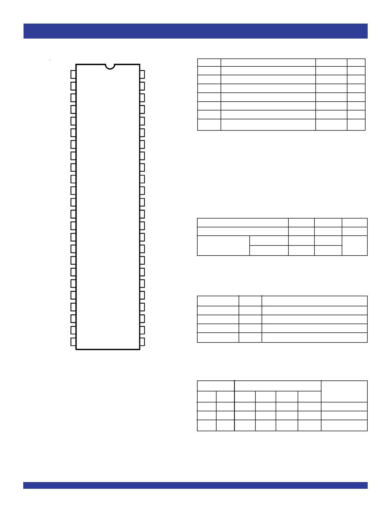
PIN CONFIGURATION
S0 1
I0A 2
I1A 3
YA 4
I0B 5
I1B 6
YB 7
GND 8
S1 9
I0E 10
I1E 11
YE 12
I0F 13
I1F 14
YF 15
GND 16
S2 17
I0I 18
I1I 19
YI 20
I0J 21
I1J 22
YJ 23
GND 24
48 VCC
47 E0
46 I0D
45 I1D
44 YD
43 I0C
42 I1C
41 YC
40 VCC
39 E1
38 I0H
37 I1H
36 YH
35 I0G
34 I1G
33 YG
32 VCC
31 E2
30 I0L
29 I1L
28 YL
27 I0K
26 I1K
25 YK
QVSOP
TOP VIEW
INDUSTRIAL TEMPERATURE RANGE
ABSOLUTE MAXIMUM RATINGS(1)
Symbol
Description
Max
Unit
VTERM(2) Supply Voltage to Ground
–0.5 to +7 V
VTERM(3) DC Switch Voltage Vs
–0.5 to +7 V
VTERM(3) DC Input Voltage VIN
–0.5 to +7 V
VAC
AC Input Voltage (pulse width ≤ 20ns)
–3
V
IOUT DC Output Current Max. Sink Current/Pin
120
mA
PMAX Maximum Power Dissipation
0.5
W
TSTG Storage Temperature
–65 to +150 °C
NOTE:
1. Stresses greater than those listed under ABSOLUTE MAXIMUM RATINGS may cause
permanent damage to the device. This is a stress rating only and functional operation
of the device at these or any other conditions above those indicated in the operational
sections of this specification is not implied. Exposure to absolute maximum rating
conditions for extended periods may affect reliability.
2. Vcc terminals.
3. All terminals except Vcc.
CAPACITANCE
(TA = +25°C, f = 1.0MHZ, VIN = 0V, VOUT = 0V)
Pins
Control Pins
Quickswitch Channels
Demux
(Switch OFF)
Mux
Typ.
Max.(1)
Unit
4
5
pF
5
7
pF
9
10
NOTE:
1. This parameter is measured at characterization but not tested.
PIN DESCRIPTION
Pin Names
I/O
Description
Ixx
I/O
Data Inputs
Sx
I
Select Input
Ex
I/O
Enable Input
Yx
I/O
Data Outputs
FUNCTION TABLE(1)
Enable
Outputs
Ex Sx
YA
YB
YC
YD
H
X
Z
Z
Z
Z
L
L
I0A
I0B
I0C
I0X
L
H
I1A
I1B
I1C
I1X
NOTE:
1. H = HIGH Voltage Level
L = LOW Voltage Level
X = Don't Care
Z = High-Impedance
Function
Disable
Select 0
Select 1
2
Share Link: