IRU1260CM 查看數據表(PDF) - International Rectifier
零件编号
产品描述 (功能)
比赛名单
IRU1260CM Datasheet PDF : 10 Pages
| |||
IRU1260
ABSOLUTE MAXIMUM RATINGS
Input Voltage (Vin) .................................................... 7V
Power Dissipation ..................................................... Internally Limited
Storage Temperature Range ...................................... -65°C To 150°C
Operating Junction Temperature Range ..................... 0°C To 150°C
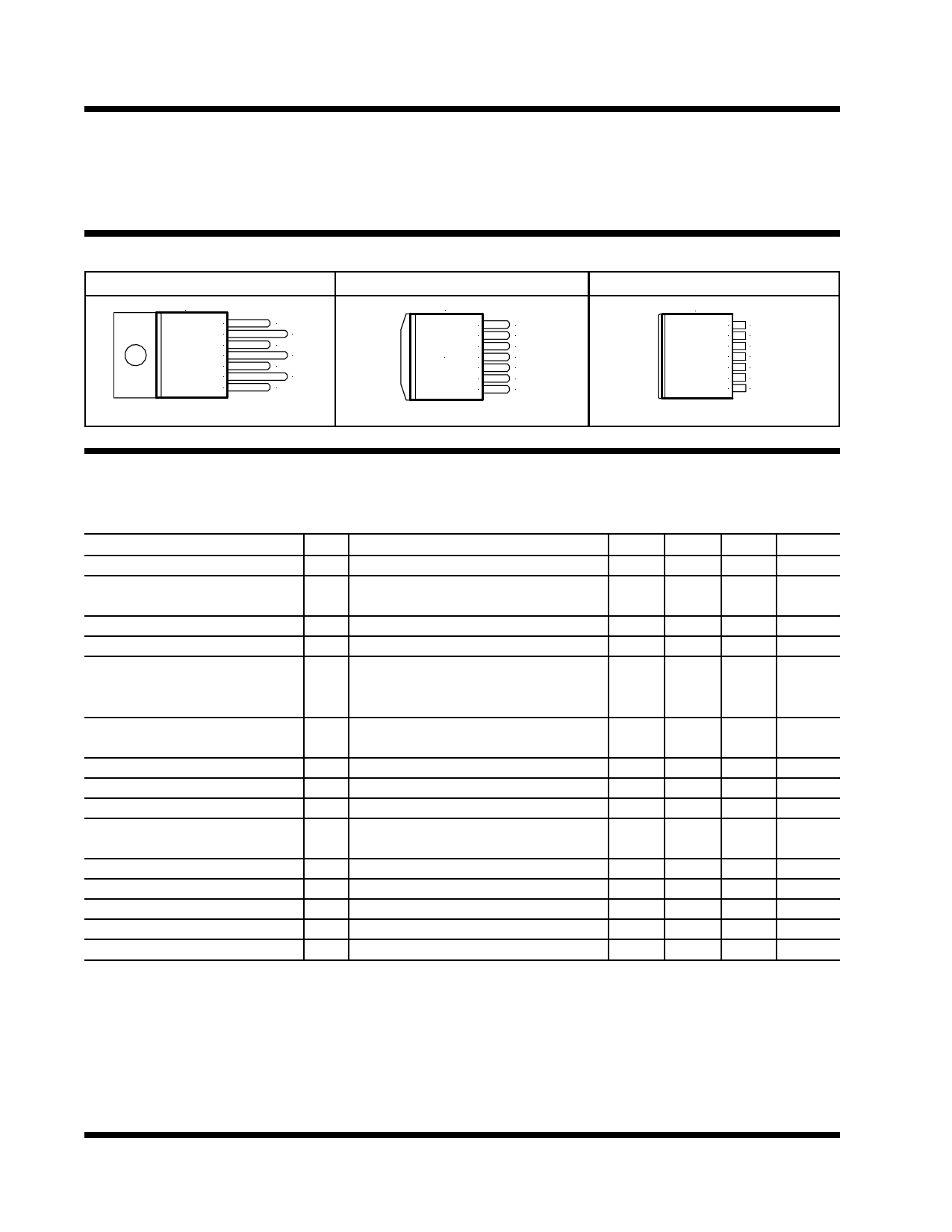
PACKAGE INFORMATION
7-PIN PLASTIC TO-220 (T)
7-PIN PLASTIC TO-263 (M)
FRONT VIEW
7
6
5
4
3
2
1
Vout1
Vin
Vout2
Gnd
Vfb2
Vfb1
Vctrl
FRONT VIEW
7
6
5
M7 4
3
2
1
Vout1
Vin
Vout2
Gnd
Vfb2
Vfb1
Vctrl
θJT=2.7$C/W, θJA=60$C/W
θJA=30$C/W for 1"sq pad
7-PIN ULTRA THIN-PAK (P)
FRONT VIEW
7
6
5
4
3
2
1
Vout1
Vin
Vout2
Gnd
Vfb2
Vfb1
Vctrl
θJA=30$C/W for 1"sq pad
ELECTRICAL SPECIFICATIONS
Unless otherwise specified, these specifications apply over Cin=1µF, Cout=10µF and Tj=0 to 150°C. Typical
values refer to Tj=25°C. IFL=6A for output #1 and IFL=1A for output #2. Vfb=Vo for both outputs. Vctrl=Vin=3.3V.
PARAMETER
Vctrl Input Voltage
Reference Voltage
Line Regulation
Load Regulation (Note 1)
Dropout Voltage (Output #2)
(Note 2)
Dropout Voltage (Output #1)
(Note 2)
Current Limit (Output #2)
Current Limit (Output #1)
Thermal Regulation
Ripple Rejection
Feedback Pin Input Current
Temperature Stability
Long Term Stability
RMS Output Noise
Minimum Load Current (Note 3)
SYM
Vref
ICL2
ICL1
IFB
TEST CONDITION
Io=10mA, Tj=25°C
Io=10mA
Io=10mA, Vout+1.3V<Vin=Vctrl<7V
10mA<Io<IFL
Io=4A, Vctrl=4.75V, Vin=3.3V
Io=3A, Vctrl=4.75V, Vin=3.3V
Io=2A, Vctrl=4.75V, Vin=3.3V
Io=1A, Vctrl=4.75V, Vin=3.3V
Io=1A, Vctrl=Vin=4.75V
∆Vo=100mV
∆Vo=100mV
30ms pulse, Io=IFL
f=120Hz, Co=25µF Tantalum,
Io=0.5 × IFL
Io=10mA
Io=10mA
Ta=125°C, 1000Hrs
Ta=25°C, 10Hz<f<10KHz
MIN TYP
3.0
1.188 1.200
1.176 1.200
0.2
0.4
0.35
0.4
6.1
1.1
0.01
70
0.02
0.5
0.3
0.003
5
MAX
1.212
1.224
1.0
0.7
0.5
0.6
1.3
0.02
1
UNITS
V
V
%
%
V
V
A
A
%/W
dB
µA
%
%
%Vo
mA
Note 1: Low duty cycle pulse testing with Kelvin con-
nections is required in order to maintain accurate data.
Note 2: Dropout voltage is defined as the minimum dif-
ferential voltage between Vin and Vout required to main-
tain regulation at Vout. It is measured when the output
voltage drops 1% below its nominal value.
Note 3: Minimum load current is defined as the mini-
mum current required at the output in order for the out-
put voltage to maintain regulation. Typically the resistor
divider values are selected such that this current is au-
tomatically maintained.
2
Rev. 1.9
07/03/01
Share Link: 