ISL8002(2013_01) 查看數據表(PDF) - Intersil
零件编号
产品描述 (功能)
比赛名单
ISL8002 Datasheet PDF : 22 Pages
| |||
ISL8002, ISL8002A, ISL80019, ISL80019A
Theory of Operation
The device is a step-down switching regulator optimized for battery
powered applications. It operates at high switching frequency (1MHz
or 2MHz) which enables the use of smaller inductors resulting in
small form factor, while also providing excellent efficiency. Further,
at light loads while in PFM mode, the regulator reduces the
switching frequency, thereby minimizing the switching loss and
maximizing battery life. The quiescent current when the output is
not loaded is typically only 35µA. The supply current is typically only
5µA when the regulator is shut down.
PWM Control Scheme
Pulling the MODE pin HI (>2.5V) forces the converter into PWM
mode, regardless of output current. The device employs the
current-mode pulse-width modulation (PWM) control scheme for
fast transient response and pulse-by-pulse current limiting. Page 5
shows the “Functional Block Diagram”. The current loop consists of
the oscillator, the PWM comparator, current sensing circuit and the
slope compensation for the current loop stability. The slope
compensation is 900mV/Ts, which changes with frequency. The
gain for the current sensing circuit is typically 300mV/A. The control
reference for the current loops comes from the error amplifier's
(EAMP) output.
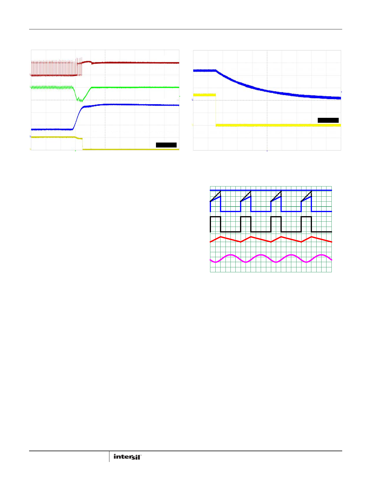
The PWM operation is initialized by the clock from the oscillator.
The P-Channel MOSFET is turned on at the beginning of a PWM
cycle and the current in the MOSFET starts to ramp up. When the
sum of the current amplifier CSA and the slope compensation
reaches the control reference of the current loop, the PWM
comparator COMP sends a signal to the PWM logic to turn off the
P-FET and turn on the N-Channel MOSFET. The N-FET stays on until
the end of the PWM cycle. Figure 50 shows the typical operating
waveforms during the PWM operation. The dotted lines illustrate
the sum of the slope compensation ramp and the current-sense
amplifier’s CSA output.
VEAMP
VCSA
DUTY
CYCLE
IL
VOUT
FIGURE 50. PWM OPERATION WAVEFORMS
The output voltage is regulated by controlling the VEAMP voltage
to the current loop. The bandgap circuit outputs a 0.6V reference
voltage to the voltage loop. The feedback signal comes from the
VFB pin. The soft-start block only affects the operation during the
start-up and will be discussed separately. The error amplifier is a
transconductance amplifier that converts the voltage error signal
to a current output. The voltage loop is internally compensated
with the 27pF and 200kΩ RC network. The maximum EAMP
voltage output is precisely clamped to 1.6V.
PFM Mode
Pulling the MODE pin LO (<0.4V) forces the converter into PFM
mode. The device enters a pulse-skipping mode at light load to
minimize the switching loss by reducing the switching frequency.
Figure 51 illustrates the skip-mode operation. A zero-cross
sensing circuit shown in Figure 51 monitors the N-FET current for
zero crossing. When 16 consecutive cycles of the inductor current
crossing zero are detected, the regulator enters the skip mode.
During the eight detecting cycles, the current in the inductor is
allowed to become negative. The counter is reset to zero when
the current in any cycle does not cross zero.
PWM
PFM
PWM
CLOCK
IL
0
VOUT
16 CYCLES
NOMINAL +1.5%
PFM CURRENT LIMIT
LOAD CURRENT
NOMINAL
NOMINAL -1.5%
FIGURE 51. SKIP MODE OPERATION WAVEFORMS
17
FN7888.1
January 7, 2013
Share Link: 