ISL8033 查看數據表(PDF) - Intersil
零件编号
产品描述 (功能)
比赛名单
ISL8033 Datasheet PDF : 18 Pages
| |||
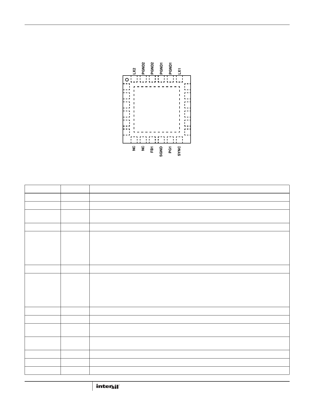
Pin Configuration
ISL8033, ISL8033A
ISL8033, ISL8033A
(24 LD QFN)
TOP VIEW
24 23 22 21 20 19
LX2 1
18 LX1
VIN2 2
17 VIN1
VIN2 3
EN2 4
16 VIN1
25
PD
15 VDD
PG2 5
14 ISET
FB2 6
13 EN1
7 8 9 10 11 12
Pin Descriptions
PIN NUMBER
1, 24
22, 23
4
5
6
7, 8
9
10
11
12
13
14
15
20, 21
SYMBOL
LX2
PGND2
EN2
PG2
FB2
NC
FB1
SGND
PG1
SYNC
EN1
ISET
VDD
PGND1
DESCRIPTION
Switching node connection for Channel 2. Connect to one terminal of inductor for VOUT2.
Negative supply for the power stage of Channel 2.
Regulator Channel 2 enable pin. Enable the output, VOUT2, when driven to high. Shutdown the VOUT2 and
discharge output capacitor when driven to low. Do not leave this pin floating.
1ms timer output. At power-up or EN HI, this output is a 1ms delayed Power-Good signal for the VOUT2 voltage.
The feedback network of the Channel 2 regulator. FB2 is the negative input to the transconductance error amplifier.
The output voltage is set by an external resistor divider connected to FB2. With a properly selected divider, the output
voltage can be set to any voltage between the power rail (reduced by converter losses) and the 0.8V reference. There
is an internal compensation to meet a typical application.
In addition, the regulator power-good and undervoltage protection circuitry use FB2 to monitor the Channel 2
regulator output voltage.
No connect pins. Please tie to GROUND.
The feedback network of the Channel 1 regulator. FB1 is the negative input to the transconductance error
amplifier. The output voltage is set by an external resistor divider connected to FB1. With a properly selected
divider, the output voltage can be set to any voltage between the power rail (reduced by converter losses) and the
0.8V reference. There is an internal compensation to meet a typical application.
In addition, the regulator power-good and undervoltage protection circuitry use FB1 to monitor the Channel 1
regulator output voltage.
System ground. Make a single point connection from these pins to PGND.
1ms timer output. At power-up or EN HI, this output is a 1ms delayed Power-Good signal for the VOUT1 voltage.
Connect to logic high or input voltage VIN. Connect to an external function generator for external Synchronization.
Negative edge trigger. Do not leave this pin floating. Do not tie this pin low (or to SGND).
Regulator Channel 1 enable pin. Enable the output, VOUT1, when driven to high. Shutdown the VOUT1 and
discharge output capacitor when driven to low. Do not leave this pin floating.
ISET is the output current limit setting of the regulators. See the “” table on page 6 for settings.
Input supply voltage for the logic. Connect VIN pin.
Negative supply for the power stage of Channel 1.
4
FN6854.2
March 24, 2011
Share Link: 