ISL8499(2005) 查看數據表(PDF) - Intersil
零件编号
产品描述 (功能)
比赛名单
ISL8499
(Rev.:2005)
(Rev.:2005)
Intersil

ISL8499 Datasheet PDF : 13 Pages
| |||
ISL8499
Absolute Maximum Ratings
V+ to GND . . . . . . . . . . . . . . . . . . . . . . . . . . . . . . . . . . . -0.3 to 4.7V
Input Voltages
NO, NC, IN (Note 2) . . . . . . . . . . . . . . . . . . . -0.3 to ((V+) + 0.3V)
Output Voltages
COM (Note 2) . . . . . . . . . . . . . . . . . . . . . . . . -0.3 to ((V+) + 0.3V)
Continuous Current NO, NC, or COM . . . . . . . . . . . . . . . . . ±300mA
Peak Current NO, NC, or COM
(Pulsed 1ms, 10% Duty Cycle, Max) . . . . . . . . . . . . . . . . ±500mA
ESD Rating:
HBM COMX . . . . . . . . . . . . . . . . . . . . . . . . . . . . . . . . . . . . . .>9kV
HBM NOX, NCX, INX, V+, GND . . . . . . . . . . . . . . . . . . . . . . .>4kV
MM COMX . . . . . . . . . . . . . . . . . . . . . . . . . . . . . . . . . . . . . .>500V
MM NOX, NCX, INX, V+, GND . . . . . . . . . . . . . . . . . . . . . . .>300V
CDM . . . . . . . . . . . . . . . . . . . . . . . . . . . . . . . . . . . . . . . . . . . .>1kV
Thermal Information
Thermal Resistance (Typical, Note 3)
θJA (°C/W)
QFN Package (Note 4). . . . . . . . . . . . . . . . . . . . . . .
70
TSSOP Package (Note 3) . . . . . . . . . . . . . . . . . . . .
150
Maximum Junction Temperature (Plastic Package) . . . . . . . 150°C
Maximum Storage Temperature Range. . . . . . . . . . . . . -65°C to 150°C
Maximum Lead Temperature (Soldering 10s) . . . . . . . . . . . . 300°C
(Lead Tips Only)
Operating Conditions
Temperature Range
ISL8499IX . . . . . . . . . . . . . . . . . . . . . . . . . . . . . . . . . -40°C to 85°C
CAUTION: Stresses above those listed in “Absolute Maximum Ratings” may cause permanent damage to the device. This is a stress only rating and operation of the
device at these or any other conditions above those indicated in the operational sections of this specification is not implied.
NOTES:
2. Signals on NC, NO, IN, or COM exceeding V+ or GND are clamped by internal diodes. Limit forward diode current to maximum current ratings.
3. θJA is measured with the component mounted on a high effective thermal conductivity test board in free air. See Tech Brief TB379 for details.
4. θJA is measured in free air with the component mounted on a high effective thermal conductivity test board with “direct attach” features. See
Tech Brief TB379.
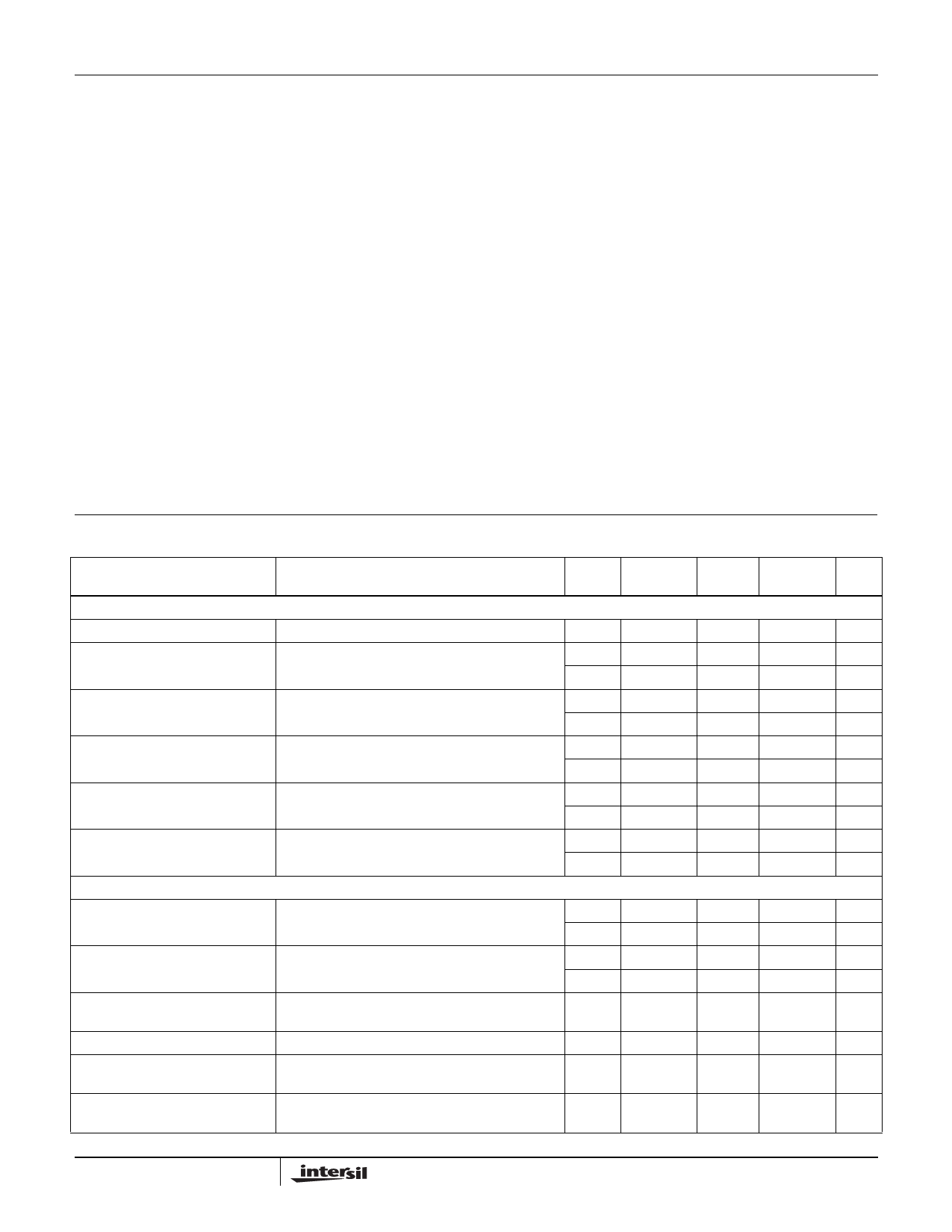
Electrical Specifications - 4.3V Supply
Test Conditions: V+ = +3.9V to +4.5V, GND = 0V, VINH = 1.6V, VINL = 0.5V (Notes 4, 6),
Unless Otherwise Specified
PARAMETER
TEST CONDITIONS
TEMP (NOTE 5)
(NOTE 5)
(°C)
MIN
TYP
MAX UNITS
ANALOG SWITCH CHARACTERISTICS
Analog Signal Range, VANALOG
Full
0
-
V+
V
ON Resistance, RON
V+ = 3.9V, ICOM = 100mA, VNO or VNC = 0V to V+,
25
-
0.25
-
Ω
(See Figure 5)
Full
-
0.28
-
Ω
RON Matching Between Channels, V+ = 3.9V, ICOM = 100mA, VNO or VNC = Voltage at
25
-
0.04
-
Ω
∆RON
max RON,(Note 9)
Full
-
0.05
-
Ω
RON Flatness, RFLAT(ON)
V+ = 3.9V, ICOM = 100mA, VNO or VNC = 0V to V+,
25
-
0.05
-
Ω
(Note 7)
Full
-
0.05
-
Ω
NO or NC OFF Leakage Current, V+ = 4.5V, VCOM = 0.3V, 3V, VNO or VNC = 3V, 0.3V
25
-50
-
50
nA
INO(OFF) or INC(OFF)
Full
-150
-
150
nA
COM ON Leakage Current,
ICOM(ON)
V+ = 4.5V, VCOM = 0.3V, 3V, or VNO or VNC = 0.3V,
25
-50
-
50
nA
3V, or Floating
Full
-150
-
150
nA
DYNAMIC CHARACTERISTICS
Turn-ON Time, tON
V+ = 3.9V, VNO or VNC = 3.0V, RL = 50Ω, CL = 35pF, 25
-
(See Figure 1, Note 8)
Full
-
15
25
ns
-
30
ns
Turn-OFF Time, tOFF
V+ = 3.9V, VNO or VNC = 3.0V, RL = 50Ω, CL = 35pF, 25
-
(See Figure 1, Note 8)
Full
-
13
23
ns
-
28
ns
Break-Before-Make Time Delay, tD V+ = 4.5V, VNO or VNC = 3.0V, RL = 50Ω, CL = 35pF, Full
2
3
-
ns
(See Figure 3, Note 8)
Charge Injection, Q
OFF Isolation
CL = 1.0nF, VG = 0V, RG = 0Ω, (See Figure 2)
25
-
-120
-
pC
RL = 50Ω, CL = 5pF, f = 100kHz, VCOM = 1VRMS,
25
-
68
-
dB
(See Figure 4)
Crosstalk (Channel-to-Channel)
RL = 50Ω, CL = 5pF, f = 100kHz, VCOM = 1VRMS,
25
-
-98
-
dB
(See Figure 6)
3
FN6111.0
January 27, 2005
Share Link: