ISL8499(2005) 查看數據表(PDF) - Intersil
零件编号
产品描述 (功能)
比赛名单
ISL8499
(Rev.:2005)
(Rev.:2005)
Intersil

ISL8499 Datasheet PDF : 13 Pages
| |||
ISL8499
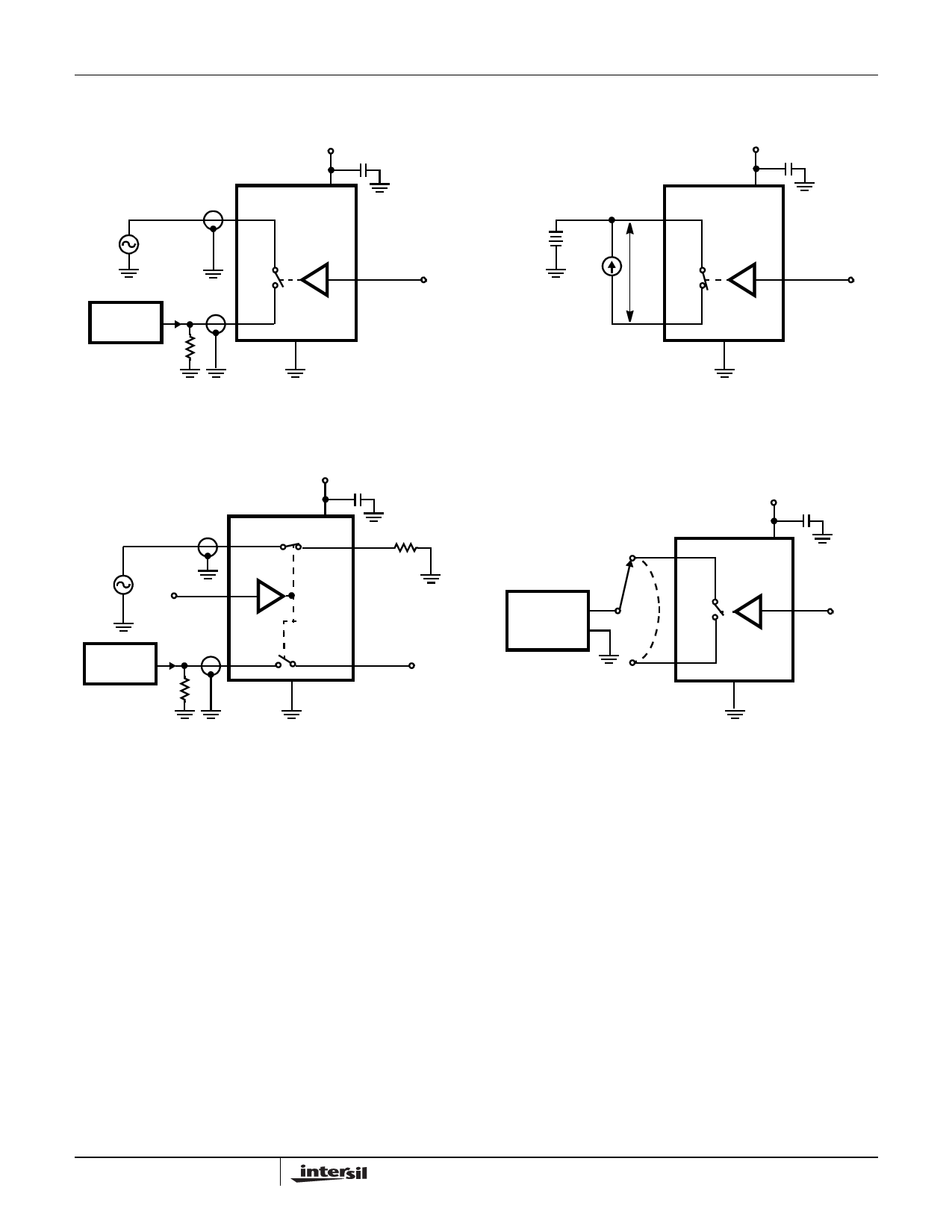
Test Circuits and Waveforms (Continued)
V+
C
SIGNAL
GENERATOR
NO or NC
IN 0V or V+
RON = V1/100mA
VNX
NO or NC
100mA
V1
V+
C
0V or V+
IN
ANALYZER
RL
COM
GND
COM
GND
FIGURE 4. OFF ISOLATION TEST CIRCUIT
FIGURE 5. RON TEST CIRCUIT
SIGNAL
GENERATOR
NO or NC
IN1
0V or V+
V+
C
COM
50Ω
ANALYZER
RL
COM
NC or NO
GND
N.C.
FIGURE 6. CROSSTALK TEST CIRCUIT
Detailed Description
The ISL8499 is a bidirectional, quad single pole/double
throw (SPDT) analog switch that offers precise switching
capability from a single 1.65V to 4.5V supply with low on-
resistance (0.24Ω) and high speed operation (tON = 15ns,
tOFF = 13ns). The device is especially well suited for
portable battery powered equipment due to its low operating
supply voltage (1.65V), low power consumption (2.7µW
max), low leakage currents (150nA max), and the tiny QFN
and TSSOP packages. The ultra low on-resistance and Ron
flatness provide very low insertion loss and distortion to
applications that require signal reproduction.
Supply Sequencing and Overvoltage Protection
With any CMOS device, proper power supply sequencing is
required to protect the device from excessive input currents
which might permanently damage the IC. All I/O pins contain
ESD protection diodes from the pin to V+ and to GND (see
7
IMPEDANCE
ANALYZER
NO or NC
V+
C
IN 0V or V+
COM
GND
FIGURE 7. CAPACITANCE TEST CIRCUIT
Figure 8). To prevent forward biasing these diodes, V+ must
be applied before any input signals, and the input signal
voltages must remain between V+ and GND. If these
conditions cannot be guaranteed, then one of the following
two protection methods should be employed.
Logic inputs can easily be protected by adding a 1kΩ
resistor in series with the input (see Figure 8). The resistor
limits the input current below the threshold that produces
permanent damage, and the sub-microamp input current
produces an insignificant voltage drop during normal
operation.
This method is not acceptable for the signal path inputs.
Adding a series resistor to the switch input defeats the
purpose of using a low RON switch, so two small signal
diodes can be added in series with the supply pins to provide
overvoltage protection for all pins (see Figure 8). These
additional diodes limit the analog signal from 1V below V+ to
FN6111.0
January 27, 2005
Share Link: