ISL8484 查看數據表(PDF) - Intersil
零件编号
产品描述 (功能)
比赛名单
ISL8484 Datasheet PDF : 13 Pages
| |||
ISL8484
Absolute Maximum Ratings
V+ to GND . . . . . . . . . . . . . . . . . . . . . . . . . . . . . . . . . . . -0.5 to 5.5V
Input Voltages
NO, NC, IN (Note 2). . . . . . . . . . . . . . . . . . . . . -0.5 to ((V+) + 0.5V)
Output Voltages
COM (Note 2). . . . . . . . . . . . . . . . . . . . . . . . . . -0.5 to ((V+) + 0.5V)
Continuous Current NO, NC, or COM . . . . . . . . . . . . . . . . . ±300mA
Peak Current NO, NC, or COM
(Pulsed 1ms, 10% Duty Cycle, Max) . . . . . . . . . . . . . . . . . . ±500mA
ESD Rating:
Human Body Model . . . . . . . . . . . . . . . . . . . . . . . . . . . . . . . .>8kV
Machine Model . . . . . . . . . . . . . . . . . . . . . . . . . . . . . . . . . . .>500V
Charged Device Model. . . . . . . . . . . . . . . . . . . . . . . . . . . . >1.4kV
Thermal Information
Thermal Resistance (Typical)
θJA (°C/W) θJC (°C/W)
10 Ld 3x3 TDFN Package (Notes 3, 4)
52
11
10 Ld MSOP Package (Note 5) . . . . . . 140
N/A
Maximum Junction Temperature (Plastic Package). . . . . . . +150°C
Maximum Storage Temperature Range . . . . . . . . . . . -65°C to +150°C
Pb-free reflow profile . . . . . . . . . . . . . . . . . . . . . . . . . .see link below
http://www.intersil.com/pbfree/Pb-FreeReflow.asp
Operating Conditions
Temperature Range . . . . . . . . . . . . . . . . . . . . . . . . . -40°C to +85°C
CAUTION: Do not operate at or near the maximum ratings listed for extended periods of time. Exposure to such conditions may adversely impact product reliability and
result in failures not covered by warranty.
NOTES:
2. Signals on NC, NO, IN, or COM exceeding V+ or GND are clamped by internal diodes. Limit forward diode current to maximum current ratings.
3. θJA is measured in free air with the component mounted on a high effective thermal conductivity test board with “direct attach” features. See
Tech Brief TB379.
4. For θJC, the “case temp” location is the center of the exposed metal pad on the package underside.
5. θJA is measured with the component mounted on a high effective thermal conductivity test board in free air. See Tech Brief TB379 for details.
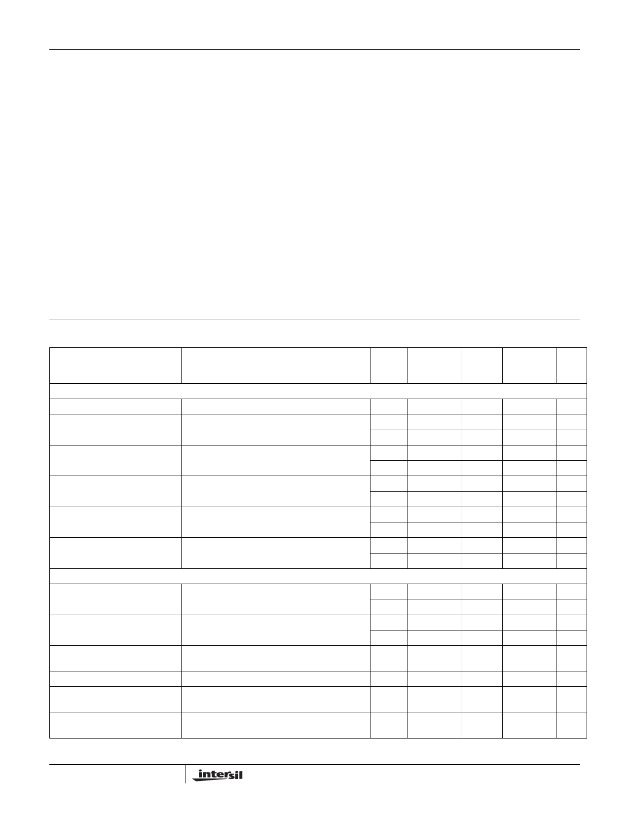
Electrical Specifications - 4.3V Supply
Test Conditions: V+ = +3.9V to +4.5V, GND = 0V, VINH = 1.4V, VINL = 0.5V (Note 6),
Unless otherwise specified.
PARAMETER
TEST CONDITIONS
TEMP
MIN
(°C) (Notes 7, 11)
ANALOG SWITCH CHARACTERISTICS
Analog Signal Range, VANALOG
Full
0
ON-Resistance, rON
V+ = 3.9V, ICOM = 100mA, VNO or VNC = 0V to V+ 25
-
(Figure 5, Note 9)
Full
-
rON Matching Between Channels, V+ = 3.9V, ICOM = 100mA, VNO or VNC = Voltage
25
-
ΔrON
at max RON (Note 9, 10)
Full
-
rON Flatness, rFLAT(ON)
V+ = 3.9V, ICOM = 100mA, VNO or VNC = 0V to V+ 25
-
(Note 8, 9)
Full
-
NO or NC OFF Leakage Current, V+ = 4.5V, VCOM = 0.3V, 3V, VNO or VNC = 3V, 0.3V 25
INO(OFF) or INC(OFF)
Full
-100
-195
COM ON Leakage Current,
ICOM(ON)
V+ = 4.5V, VCOM = 0.3V, 3V, or VNO or VNC = 0.3V, 25
3V, or Floating
Full
-100
-195
DYNAMIC CHARACTERISTICS
Turn-ON Time, tON
V+ = 3.9V, VNO or VNC = 3.0V, RL = 50Ω, CL = 35pF 25
-
(Figure 1)
Full
-
Turn-OFF Time, tOFF
V+ = 3.9V, VNO or VNC = 3.0V, RL = 50Ω, CL = 35pF 25
-
(Figure 1)
Full
-
Break-Before-Make Time Delay, tD V+ = 4.5V, VNO or VNC = 3.0V, RL = 50Ω, CL = 35pF Full
-
(Figure 3)
Charge Injection, Q
OFF Isolation
CL = 1.0nF, VG = 0V, RG = 0Ω (Figure 2)
25
-
RL = 50Ω, CL = 5pF, f = 100kHz, VCOM = 1VRMS
25
-
(Figure 4)
Crosstalk (Channel-to-Channel) RL = 50Ω, CL = 5pF, f = 100kHz, VCOM = 1VRMS
25
-
(Figure 6)
TYP
-
0.30
0.35
0.06
0.08
0.03
0.04
-
-
-
-
40
50
20
30
8
170
62
-85
MAX
(Notes 7, 11) UNITS
V+
V
0.5
Ω
0.7
Ω
0.07
Ω
0.08
Ω
0.15
Ω
0.15
Ω
100
nA
195
nA
100
nA
195
nA
-
ns
-
ns
-
ns
-
ns
-
ns
-
pC
-
dB
-
dB
3
FN6128.5
May 12, 2008
Share Link: 