IT1 查看數據表(PDF) - HIROSE ELECTRIC
零件编号
产品描述 (功能)
比赛名单
IT1 Datasheet PDF : 17 Pages
| |||
The product information in this catalog is for reference only. Please request the Engineering Drawing for the most current and accurate design information.
All non-RoHS products have been discontinued, or will be discontinued soon. Please chIeTc1k tSheeprrioedsu●ctsHsitgathus SonpteheeHdir,oMseawtecbshiteedRo-HImS speaerdchaantcwew,w.Phiarorsae-lcleonlnBecotoarsr.dco-mto, o-rbcoonatradct yCouornHnireoscetosarleSs ryesprteesmentative.
2. Recommended Design Guidelines
2-1 Solder Land Pattern
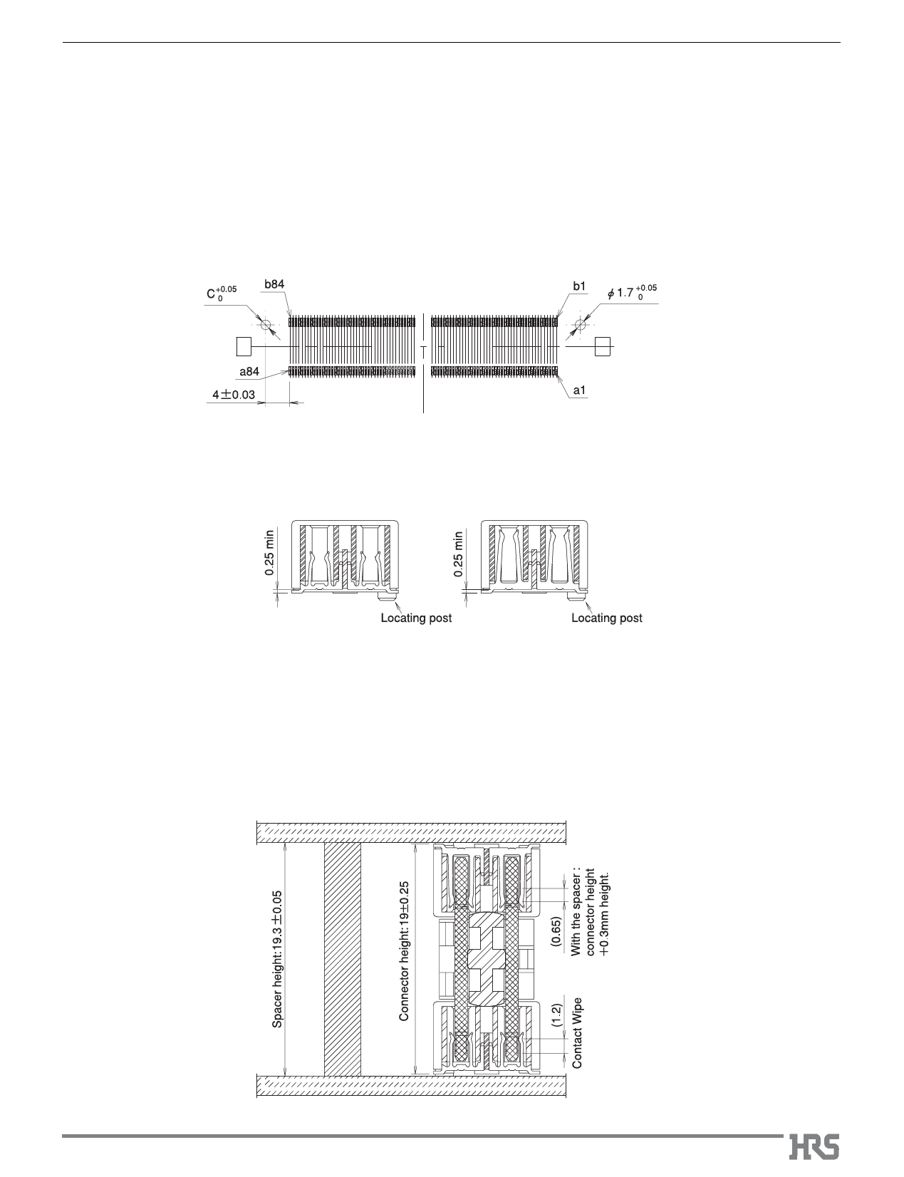
When placing the receptacles on the Printed Circuit Boards using automatic mounting equipment or manually, assure that the
correct diameters of the holes (Fig. 1) are through the entire thickness of the board.
SLocating post hole diameterS
The contacts of receptacle assembly are exposed on the bottom surfaces. The exposed areas of the contacts are a distance
of 0.25 mm minimum from the surface of the Printed Circuit Board, on which the receptacle assembly is placed (Fig.2).
Consideration should be taken not to place or assure insulation of conductive traces under the receptacle assemblies.
Refer to the separate drawings for recommended solder land pattern dimensions of the receptacle, and signals and ground
connection diagram of the transmission module.
(mm)
Automatic placement / (Locating post hole diameter) C dimension: 1.7 mm
Manual placement
/ (Locating post hole diameter) C dimension: 1.6 mm
/ A position accuracy of +-0.03 should be exercised from the
center of the hole to contact Number 84.
Fig. 1 IT1-168S-SV Recommended Solder Land Pattern
Contact_A
Contact_B
Fig. 2 Cross section of IT1 receptacle
2-2 Board-to-Board Spacer heights
The two parallel boards connected by the IT1 connectors should be fastened to additional spacers between them.
Fig. 3 indicates the connector height tolerance and the spacer’s height.
When designing the spacer’s height, consideration should be given to the solder paste thickness and any other features,
which may affect the full mating of the connector.
Fig. 3 indicates design dimensions for the 19 mm board-to-board distance.
(mm)
Fig. 3
A303
Share Link: 