IW4043B 查看數據表(PDF) - IK Semicon Co., Ltd
零件编号
产品描述 (功能)
比赛名单
IW4043B Datasheet PDF : 6 Pages
| |||
TECHNICAL DATA
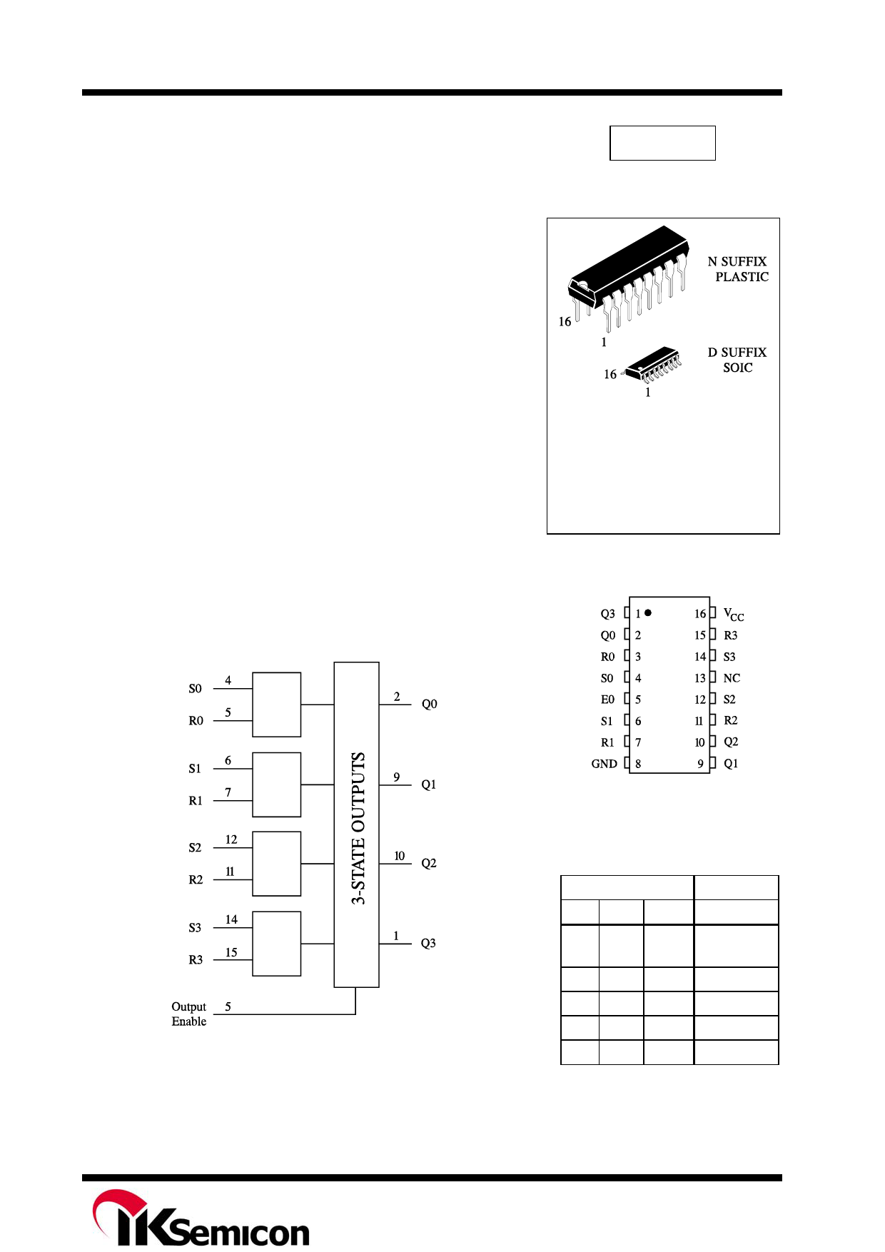
Quad 3-State R/S Latches
High-Voltage Silicon-Gate CMOS
IW4043B
The IW4043B types are quad cross-coupled 3-state CMOS NOR
latces. Each latch has a separate Q output and individual SET and RESET
inputs. The Q outputs are controlled by a common ENABLE input. A
logic “1” or high on the ENABLE input connects the latch states to the Q
outputs. A logic “0” or low on the ENABLE input disconnects the latch
states from the Q outputs, resulting in an open circuit condition on the Q
outputs. The open circuit feature allows common busing of the outputs.
• Operating Voltage Range: 3.0 to 18 V
• Maximum input current of 1 μA at 18 V over full package-temperature
range; 100 nA at 18 V and 25°C
• Noise margin (over full package temperature range):
1.0 V min @ 5.0 V supply
2.0 V min @ 10.0 V supply
2.5 V min @ 15.0 V supply
ORDERING INFORMATION
IW4043BN Plastic
IW4043BD SOIC
TA = -55° to 125° C for all packages
PIN ASSIGNMENT
LOGIC DIAGRAM
PIN 13 = NO CONNECTION
PIN 16=VCC
PIN 8= GND
FUNCTION TABLE
Inputs
S R OE
XX L
LL H
LH H
HL H
HH H
X = don’t care
Outputs
Q
High
Impedance
No change
L
H
H
Rev. 00
Share Link: 