K4S640832D-TC/L80 查看數據表(PDF) - Samsung
零件编号
产品描述 (功能)
比赛名单
K4S640832D-TC/L80 Datasheet PDF : 10 Pages
| |||
K4S640832D
AC OPERATING TEST CONDITIONS(VDD = 3.3V ± 0.3V, TA = 0 to 70°C)
Parameter
Input levels (Vih/Vil)
Input timing measurement reference level
Input rise and fall time
Output timing measurement reference level
Output load condition
Value
2.4/0.4
1.4
tr/tf = 1/1
1.4
See Fig. 2
3.3V
Output
870Ω
1200Ω
50pF
VOH (DC) = 2.4V, IOH = -2mA
VOL (DC) = 0.4V, IOL = 2mA
Output
CMOS SDRAM
Unit
V
V
ns
V
Z0 = 50Ω
Vtt = 1.4V
50Ω
50pF
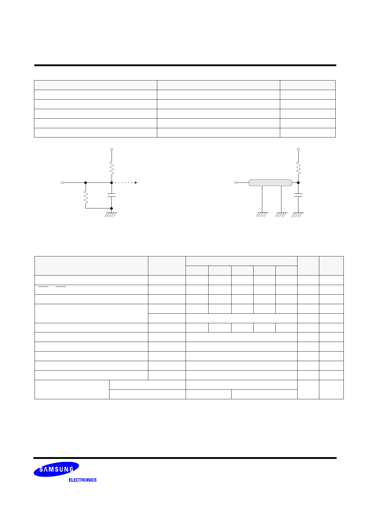
(Fig. 1) DC output load circuit
(Fig. 2) AC output load circuit
OPERATING AC PARAMETER
(AC operating conditions unless otherwise noted)
Parameter
Symbol
Version
Unit
- 75
- 80
- 1H - 1L
-10
Row active to row active delay
tRRD(min)
15
16
20
20
20
ns
RAS to CAS delay
tRCD(min)
20
20
20
20
24
ns
Row precharge time
tRP(min)
20
20
20
20
24
ns
Row active time
tRAS(min)
45
48
50
50
50
ns
tRAS(max)
100
us
Row cycle time
tRC(min)
65
68
70
70
80
ns
Last data in to row precharge
tRDL(min)
2
CLK
Last data in to Active delay
tDAL(min)
2 CLK + 20 ns
-
Last data in to new col. address delay
tCDL(min)
1
CLK
Last data in to burst stop
tBDL(min)
1
CLK
Col. address to col. address delay
tCCD(min)
1
CLK
Number of valid output data
CAS latency=3
CAS latency=2
2
ea
-
1
Notes : 1. The minimum number of clock cycles is determined by dividing the minimum time required with clock cycle time
and then rounding off to the next higher integer.
2. Minimum delay is required to complete write.
3. All parts allow every cycle column address change.
4. In case of row precharge interrupt, auto precharge and read burst stop.
5. For -80/1H/1L/10, tRDL=1CLK and tDAL=1CLK+20ns is also supported .
SAMSUNG recommands tRDL=2CLK and tDAL=2CLK + 20ns.
Note
1
1
1
1
1
2,5
5
2
2
3
4
Rev. 0.0 May 1999
Share Link: 