L4937 查看數據表(PDF) - STMicroelectronics
零件编号
产品描述 (功能)
比赛名单
L4937 Datasheet PDF : 9 Pages
| |||
L4937N
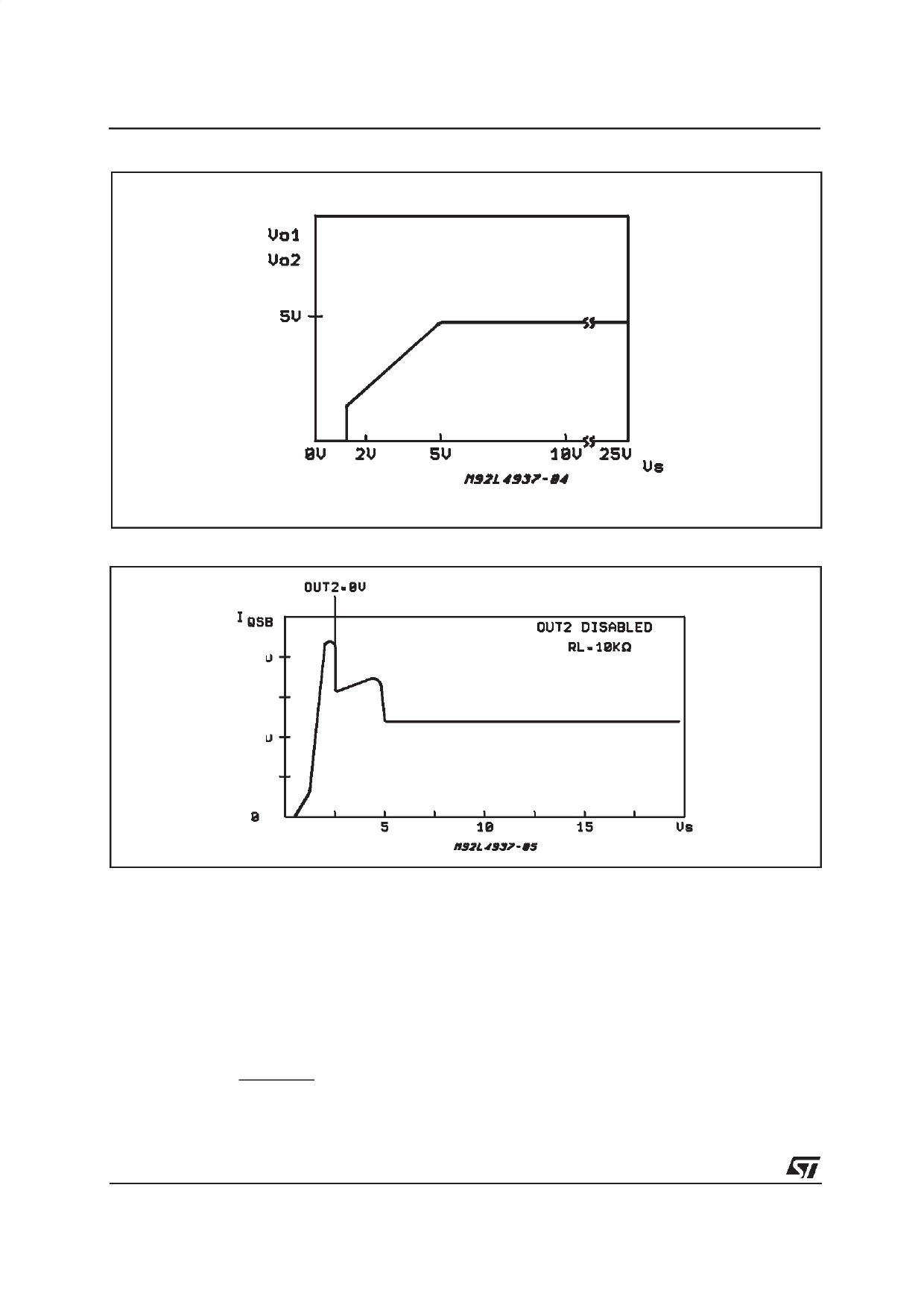
Figure 1 : Output Voltage vs. Input Voltage.
Figure 2 : Quiescent Current vs. Supply Voltage.
400
200
RESET CIRCUIT
Theblock circuit diagramof the resetcircuit is shown
in fig.3. Thereset circuit supervisesthe standbyout-
put voltage. The reset threshold of 4.7V is defined
by the internal reference voltage and the standby
output divider.
The reset pulse delay time tRD, is defined by the
charge time of an external capacitor CT :
tRD =
CT x 2V
2µA
The reaction time of the reset circuit dependson the
discharge time limitation of the reset capacitor CT
and is proportional to the value of CT.
The reaction time of the reset circuit increases the
noise immunity. In fact, if the standbyoutput voltage
drops below the reset threshold for a time shorter
than the reaction time tRR, no reset output variation
occurs. The nominal reset delay is generated for
standby output voltage drops longer than the time
necessary for the complete discharging of the ca-
pacitor CT. This time is typically equal to 50µs if CT
= 100nF. The typical reset output waveforms are
shown in fig.
6/9
Share Link: 