LT1175 查看數據表(PDF) - Linear Technology
零件编号
产品描述 (功能)
比赛名单
LT1175 Datasheet PDF : 18 Pages
| |||
LT1175
Applications Information
TA = Maximum ambient temperature
TMAX = Maximum LT1175 die temperature (125°C for
commercial and industrial grades)
θJA = LT1175 thermal resistance, junction to ambient
VIN = Maximum continuous input voltage at maximum
load current
ILOAD = Maximum load current
Example: LT1175S8 with ILOAD = 200mA, VOUT = 5V,
VIN = 7V, TA = 60°C. Maximum die temperature for the
LT1175S8 is 125°C. Thermal resistance from Table 2 is
found to be 80°C/W.
Die Temperature = 60 + 80 (0.2A)(8 – 5) = 108°C
Maximum Power Dissipation = 125 – 60 = 0.81W
80
( ) Maximum Continuous
Input Voltage
= 125 – 60 + 5 = 9V
(for Thermal Considerations) 80 0.2
between the input and output of the regulator. Reverse
voltages between input and output above 1V will damage
the regulator if large currents are allowed to flow. Simply
disconnecting the input source with the output held up
will not cause damage even though the input-to-output
voltage will become slightly reversed.
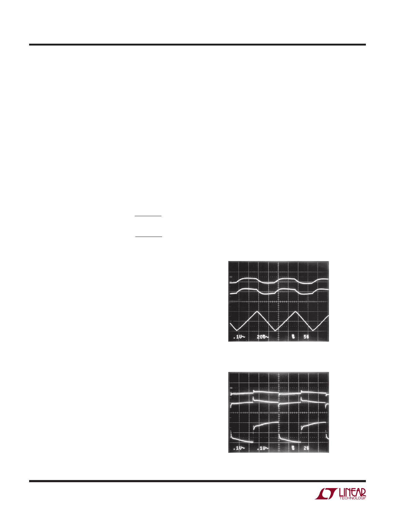
High Frequency Ripple Rejection
The LT1175 will sometimes be powered from switching
regulators that generate the unregulated or quasi-regulated
input voltage. This voltage will contain high frequency ripple
that must be rejected by the linear regulator. Special care
was taken with the LT1175 to maximize high frequency
ripple rejection, but as with any micropower design,
rejection is strongly affected by ripple frequency. The
graph in the Typical Performance Characteristics section
shows 60dB rejection at 1kHz, but only 15dB rejection at
100kHz for the 5V part. Photographs in Figures 4a and 4b
show actual output ripple waveforms with square wave
and triwave input ripple.
Output Voltage Reversal
The LT1175 is designed to tolerate an output voltage
reversal of up to 2V. Reversal might occur, for instance,
if the output was shorted to a positive 5V supply. This
would almost surely destroy IC devices connected to the
negative output. Reversal could also occur during start-
up if the positive supply came up first and loads were
connected between the positive and negative supplies.
For these reasons, it is always good design practice to
add a reverse biased diode from each regulator output to
ground to limit output voltage reversal. The diode should
be rated to handle full negative load current for start-up
situations, or the short-circuit current of the positive supply
if supply-to-supply shorts must be tolerated.
Input Voltage Lower Than Output
Linear Technology’s positive low dropout regulators
LT1121 and LT1129, will not draw large currents if the
input voltage is less than the output. These devices use a
lateral PNP power transistor structure that has 40V emitter
base breakdown voltage. The LT1175, however, uses an
NPN power transistor structure that has a parasitic diode
OUTPUT
20mV/DIV
INPUT
RIPPLE
100mV/DIV
OUTPUT
100mV/DIV
INPUT
RIPPLE
100mV/DIV
12
COUT = 4.7µF TANT
COUT = 1µF TANT
f = 50kHz
5µs/DIV
Figure 4a.
1175 F04a
COUT = 4.7µF TANT
COUT = 1µF TANT
f = 100kHz
2µs/DIV
Figure 4b.
1175 F04b
1175fe
Share Link: 