LT1965IT-TRPBF(V2) 查看數據表(PDF) - Linear Technology
零件编号
产品描述 (功能)
比赛名单
LT1965IT-TRPBF Datasheet PDF : 16 Pages
| |||
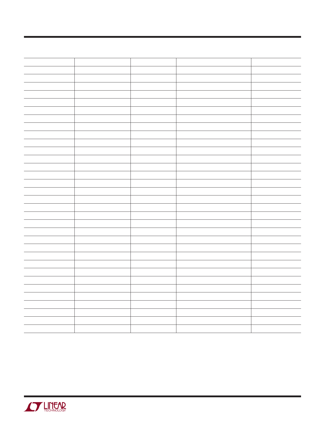
LT1965
ELECTRICAL CHARACTERISTICS The ● denotes the specifications which apply over the full operating
temperature range, otherwise specifications are at TA = 25°C. (Note 3)
PARAMETER
CONDITIONS
MIN TYP MAX UNITS
Minimum Input Voltage (Notes 4, 12)
ADJ Pin Voltage (Notes 4, 5)
Line Regulation (Note 4)
Load Regulation
Dropout Voltage
VIN = VOUT(NOMINAL)
(Notes 6, 7, 12)
GND Pin Current
VIN = VOUT(NOMINAL) + 1V
(Notes 6, 8)
Output Voltage Noise
ADJ Pin Bias Current (Notes 4, 9)
ILOAD = 0.5A
ILOAD = 1.1A
VIN = 2.1V, ILOAD = 1mA
2.3V < VIN < 20V, 1mA < ILOAD < 1.1A
ΔVIN = 2.1V to 20V, ILOAD = 1mA
VIN = 2.3V, ΔILOAD = 1mA to 1.1A
VIN = 2.3V, ΔILOAD = 1mA to 1.1A
ILOAD = 1mA
ILOAD = 1mA
ILOAD = 100mA
ILOAD = 100mA
ILOAD = 500mA
ILOAD = 500mA
ILOAD = 1.1A
ILOAD = 1.1A
ILOAD = 0mA
ILOAD = 1mA
ILOAD = 100mA
ILOAD = 500mA
ILOAD = 1.1A
COUT = 10μF, ILOAD = 1.1A, BW = 10Hz to 100kHz
1.65
V
●
1.8
2.3
V
1.182 1.20 1.218
V
● 1.164 1.20 1.236
V
●
3
8
mV
4.25
8
mV
●
16
mV
0.05 0.08
V
●
0.14
V
0.10 0.175
V
●
0.28
V
0.19 0.25
V
●
0.36
V
0.29 0.36
V
●
0.49
V
●
0.5
1.1
mA
●
0.6
1.5
mA
●
2.2
5.5
mA
●
8.2
20
mA
●
21
40
mA
40
μVRMS
1.3
4.5
μA
Shutdown Threshold
⎯S⎯H⎯D⎯N Pin Current (Note 10)
Quiescent Current in Shutdown
Ripple Rejection
Current Limit
Input Reverse Leakage Current
Reverse Output Current (Note 11)
VOUT = Off to On
VOUT = On to Off
V⎯S⎯H⎯D⎯N = 0V
V⎯S⎯H⎯D⎯N = 20V
VIN = 6V, V⎯S⎯H⎯D⎯N = 0V
VIN – VOUT = 1.5V (AVG), VRIPPLE = 0.5VP-P,
fRIPPLE = 120Hz, ILOAD = 0.75A
VIN = 7V, VOUT = 0
VIN = VOUT(NOMINAL) + 1V, ΔVOUT = -0.1V (Note 6)
VIN = –20V, VOUT = 0
VOUT = 1.2V, VIN < 1.2V (Note 4)
●
0.85
2
V
● 0.2
0.45
V
0.01
1
μA
5.5
10
μA
0.01
1
μA
57
75
dB
2
A
● 1.2
A
1
mA
175
400
μA
Note 1: Stresses beyond those listed under Absolute Maximum Ratings
may cause permanent damage to the device. Exposure to any Absolute
Maximum Rating condition for extended periods may affect device
reliability and lifetime.
Note 2: Absolute maximum input to output differential voltage is not
achievable with all combinations of rated IN pin and OUT pin voltages.
With the IN pin at 22V, the OUT pin may not be pulled below 0V. The total
measured voltage from IN to OUT must not exceed ±22V.
Note 3: The LT1965 is tested and specified under pulse load conditions
such that TJ ≅ TA. The LT1965E is 100% tested at TA = 25°C. Performance
at –40°C and 125°C is assured by design, characterization, and correlation
with statistical process controls. The LT1965I is guaranteed over the full
–40°C to 125°C operating junction temperature range.
Note 4: The LT1965 is tested and specified for these conditions with the
ADJ connected to the OUT pin.
Note 5: Maximum junction temperature limits operating conditions. The
regulated output voltage specification does not apply for all possible
combinations of input voltage and output current. Limit the output current
range if operating at the maximum input voltage. Limit the input-to-output
voltage differential if operating at the maximum output current.
Note 6: To satisfy minimum input voltage requirements, the LT1965 is
tested and specified for these conditions with an external resistor divider
(bottom 4.02k, top 4.32k) for an output voltage of 2.5V. The external
resistor divider adds 300μA of output DC load current.
Note 7: Dropout voltage is the minimum input-to-output voltage
differential needed to maintain regulation at a specified output current. In
dropout, the output voltage equals: (VIN – VDROPOUT)
Note 8: GND pin current is tested with VIN = VOUT(NOMINAL) + 1V and a
current source load. GND pin current increases slightly in dropout. See
GND pin current curves in the Typical Performance Characteristics section.
1965f
3
Share Link: 