LT3024EDE 查看數據表(PDF) - Linear Technology
零件编号
产品描述 (功能)
比赛名单
LT3024EDE Datasheet PDF : 20 Pages
| |||
LT3024
APPLICATIONS INFORMATION
The LT3024 is a dual 100mA/500mA low dropout regulator
with micropower quiescent current and shutdown. The
device is capable of supplying 100mA from Output 2 at a
dropout voltage of 300mV. Output 1 delivers 500mA at a
dropout voltage of 300mV. The two regulators have com-
mon VIN and GND pins and are thermally coupled, however,
the two outputs of the LT3024 operate independently. They
can be shut down independently and a fault condition on
one output will not affect the other output electrically.
Output voltage noise can be lowered to 20μVRMS over a
10Hz to 100kHz bandwidth with the addition of a 0.01μF
reference bypass capacitor. Additionally, the reference
bypass capacitor will improve transient response of the
regulator, lowering the settling time for transient load
conditions. The low operating quiescent current (30μA per
output) drops to less than 1μA in shutdown. In addition to
the low quiescent current, the LT3024 regulator incorpo-
rates several protection features which make it ideal for
use in battery-powered systems. The device is protected
against both reverse input and reverse output voltages.
In battery backup applications where the output can be
held up by a backup battery when the input is pulled to
ground, the LT3024 acts like it has a diode in series with
its output and prevents reverse current flow. Additionally,
in dual supply applications where the regulator load is
returned to a negative supply, the output can be pulled
below ground by as much as 20V and still allow the device
to start and operate.
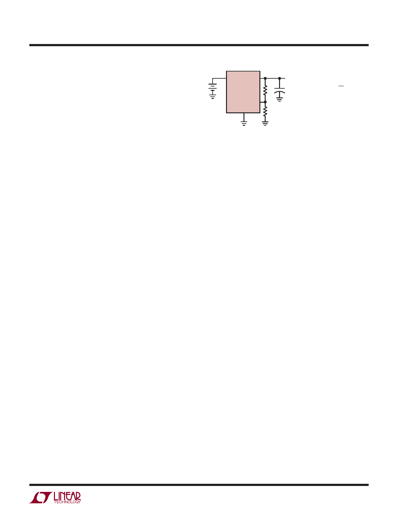
Adjustable Operation
The LT3024 has an output voltage range of 1.22V to 20V.
The output voltage is set by the ratio of two external resis-
tors as shown in Figure 1. The device servos the output
to maintain the corresponding ADJ pin voltage at 1.22V
referenced to ground. The current in R1 is then equal to
1.22V/R1 and the current in R2 is the current in R1 plus
the ADJ pin bias current. The ADJ pin bias current, 30nA
at 25°C, flows through R2 into the ADJ pin. The output
voltage can be calculated using the formula in Figure 1. The
IN OUT1/OUT2
VIN
LT3024
ADJ1/ADJ2
GND
+
R2
VOUT
( )( ) VOUT
=
⎛
1.22V ⎝⎜ 1+
R2⎞
R1⎠⎟
+
IADJ
R2
VADJ = 1.22V
IADJ = 30nA AT 25°C
R1
OUTPUT RANGE = 1.22V TO 20V
3024 F01
Figure 1. Adjustable Operation
value of R1 should be no greater than 250k to minimize
errors in the output voltage caused by the ADJ pin bias
current. Note that in shutdown the output is turned off and
the divider current will be zero. Curves of ADJ Pin Voltage
vs Temperature and ADJ Pin Bias Current vs Temperature
appear in the Typical Performance Characteristics.
The device is tested and specified with the ADJ pin tied to
the corresponding OUT pin for an output voltage of 1.22V.
Specifications for output voltages greater than 1.22V will
be proportional to the ratio of the desired output voltage
to 1.22V: VOUT/1.22V. For example, load regulation on
Output 2 for an output current change of 1mA to 100mA
is –1mV typical at VOUT = 1.22V. At VOUT = 12V, load
regulation is:
(12V/1.22V)(–1mV) = –9.8mV
Bypass Capacitance and Low Noise Performance
The LT3024 regulator may be used with the addition of a
bypass capacitor from VOUT to the corresponding BYP pin
to lower output voltage noise. A good quality low leakage
capacitor is recommended. This capacitor will bypass the
reference of the regulator, providing a low frequency noise
pole. The noise pole provided by this bypass capacitor will
lower the output voltage noise to as low as 20μVRMS with
the addition of a 0.01μF bypass capacitor. Using a bypass
capacitor has the added benefit of improving transient
response. With no bypass capacitor and a 10μF output
capacitor, a 10mA to 100mA load step on Output 2 will settle
to within 1% of its final value in less than 100μs. With the
addition of a 0.01μF bypass capacitor, the output will stay
3024fa
13
Share Link: 