LT3024IFE 查看數據表(PDF) - Linear Technology
零件编号
产品描述 (功能)
比赛名单
LT3024IFE Datasheet PDF : 20 Pages
| |||
LT3024
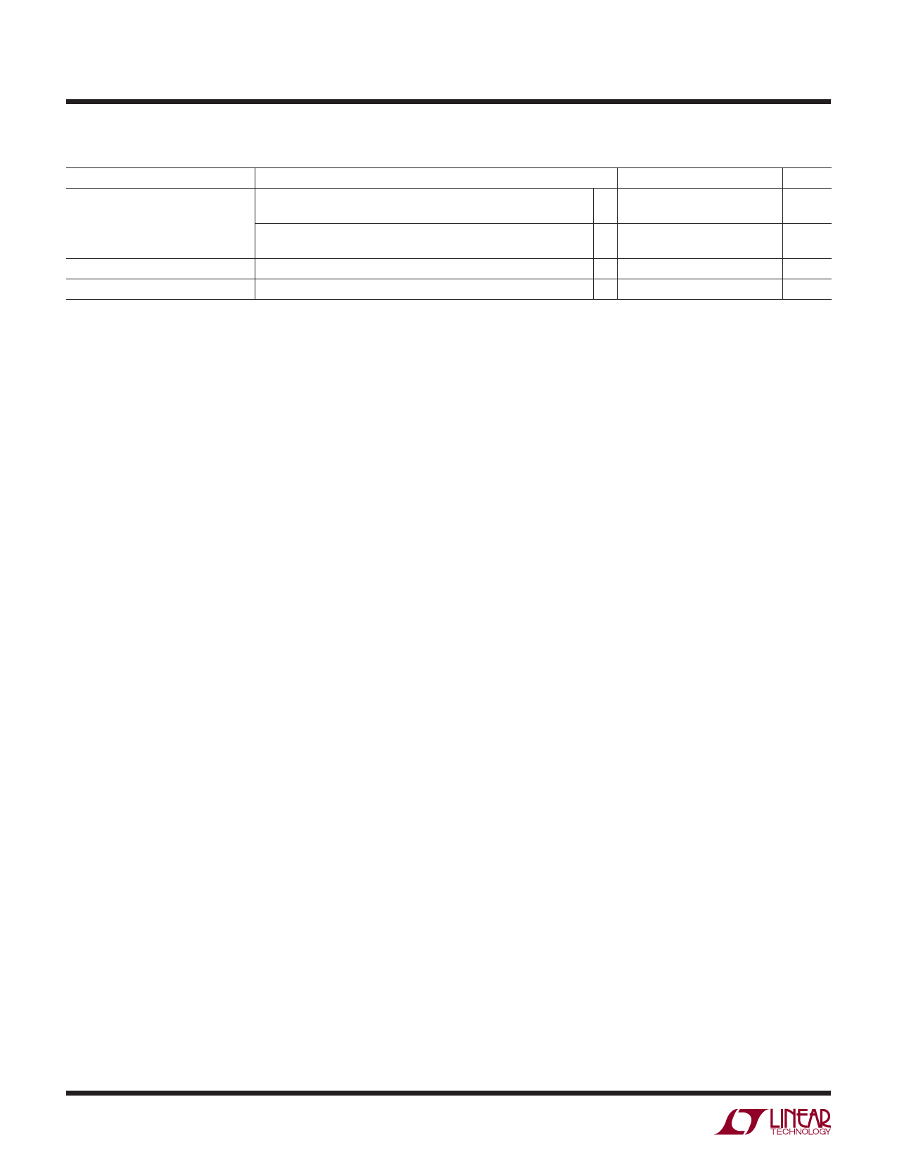
ELECTRICAL CHARACTERISTICS The l denotes the specifications which apply over the full operating
temperature range, otherwise specifications are at TA = 25°C. (Note 2)
PARAMETER
CONDITIONS
MIN
TYP
MAX
Current Limit
Input Reverse Leakage Current
Reverse Output Current (Notes 3,10)
Output 2, VIN = 7V, VOUT = 0V
VIN = 2.3V, ΔVOUT = –0.1V
Output 1, VIN = 7V, VOUT = 0V
VIN = 2.3V, ΔVOUT = –0.1V
VIN = –20V, VOUT = 0V
VOUT = 1.22V, VIN < 1.22V
200
l 110
700
l 520
l
1
5
10
UNITS
mA
mA
mA
mA
mA
μA
Note 1: Stresses beyond those listed under Absolute Maximum Ratings
may cause permanent damage to the device. Exposure to any Absolute
Maximum Rating condition for extended periods may affect device
reliability and lifetime.
Note 2: The LT3024 is tested and specified under pulse load conditions
such that TJ ≅ TA. The LT3024E is 100% tested at TA = 25°C. Performance
at – 40°C and 125°C is assured by design, characterization and correlation
with statistical process controls. The LT3024I is guaranteed over the full
–40°C to 125°C operating junction temperature range.
Note 3: The LT3024 is tested and specified for these conditions with the
ADJ1/ADJ2 pin connected to the corresponding OUT1/OUT2 pin.
Note 4: Operating conditions are limited by maximum junction
temperature. The regulated output voltage specification will not apply
for all possible combinations of input voltage and output current. When
operating at maximum input voltage, the output current range must be
limited. When operating at maximum output current, the input voltage
range must be limited.
Note 5: To satisfy requirements for minimum input voltage, the LT3024 is
tested and specified for these conditions with an external resistor divider
(two 250k resistors) for an output voltage of 2.44V. The external resistor
divider will add a 5μA DC load on the output.
Note 6: Dropout voltage is the minimum input to output voltage differential
needed to maintain regulation at a specified output current. In dropout, the
output voltage will be equal to: VIN – VDROPOUT.
Note 7: GND pin current is tested with VIN = 2.44V and a current source
load. This means the device is tested while operating in its dropout region
or at the minimum input voltage specification. This is the worst-case GND
pin current. The GND pin current will decrease slightly at higher input
voltages. Total GND pin current is equal to the sum of GND pin currents
from Output 1 and Output 2.
Note 8: ADJ1 and ADJ2 pin bias current flows into the pin.
Note 9: SHDN1 and SHDN2 pin current flows into the pin.
Note 10: Reverse output current is tested with the IN pin grounded and the
OUT pin forced to the rated output voltage. This current flows into the OUT
pin and out the GND pin.
Note 11: For the LT3024 dropout voltage will be limited by the minimum
input voltage specification under some output voltage/load conditions.
See the curve of Minimum Input Voltage in the Typical Performance
Characteristics.
3024fa
4
Share Link: 