LT3684EDD 查看數據表(PDF) - Linear Technology
零件编号
产品描述 (功能)
比赛名单
LT3684EDD Datasheet PDF : 24 Pages
| |||
LT3684
ABSOLUTE MAXIMUM RATINGS
(Note 1)
VIN, RUN/SS Voltage.................................................36V
BOOST Pin Voltage ...................................................56V
BOOST Pin Above SW Pin.........................................30V
FB, RT, VC Voltage.......................................................5V
BIAS, PG, BD Voltage................................................30V
Maximum Junction Temperature .......................... 125°C
Operating Temperature Range (Note 2)
LT3684E............................................... –40°C to 85°C
LT3684I ............................................. –40°C to 125°C
Storage Temperature Range................... –65°C to 150°C
Lead Temperature (Soldering, 10 sec)
(MSE Only) ....................................................... 300°C
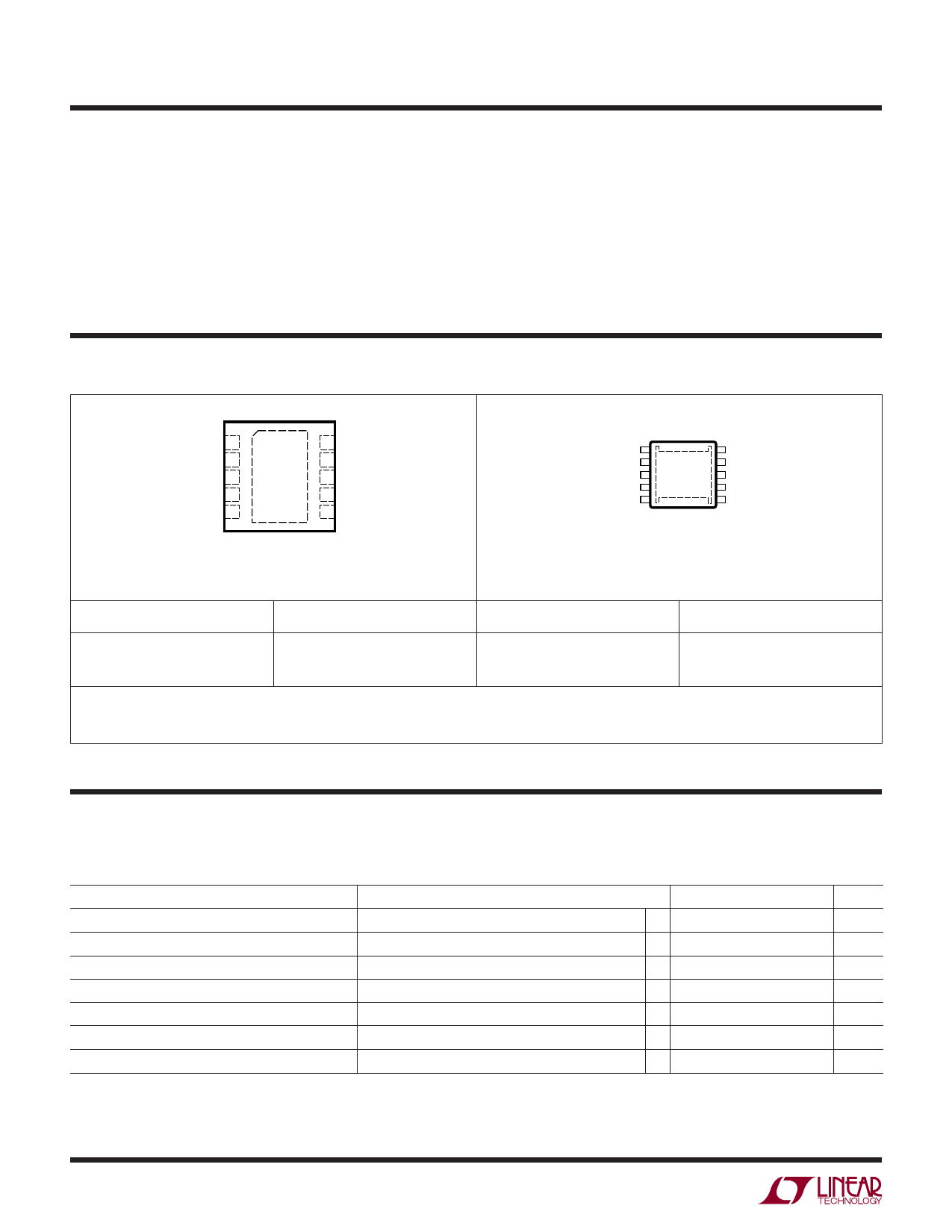
PACKAGE/ORDER INFORMATION
TOP VIEW
BD 1
BOOST 2
SW 3
VIN 4
RUN/SS 5
10 RT
9 VC
11
8 FB
7 BIAS
6 PG
DD PACKAGE
10-LEAD (3mm × 3mm) PLASTIC DFN
TJMAX = 125°C, θJA = 45°C/W, θJC = 10°C/W
EXPOSED PAD (PIN 11) IS GND, MUST BE SOLDERED TO PCB
BD 1
BOOST 2
SW 3
VIN 4
RUN/SS 5
TOP VIEW
11
10 RT
9 VC
8 FB
7 BIAS
6 PG
MSE PACKAGE
10-LEAD PLASTIC MSOP
TJMAX = 125°C, θJA = 45°C/W, θJC = 10°C/W
EXPOSED PAD (PIN 11) IS GND, MUST BE SOLDERED TO PCB
ORDER PART NUMBER DD PART MARKING* ORDER PART NUMBER MSE PART MARKING*
LT3684EDD
LT3684IDD
LCVT
LCVT
LT3684EMSE
LT3684IMSE
LTCVS
LTCVS
Order Options Tape and Reel: Add #TR
Lead Free: Add #PBF Lead Free Tape and Reel: Add #TRPBF
Lead Free Part Marking: http://www.linear.com/leadfree/
Consult LTC Marketing for parts specified with wider operating temperature ranges. *The temperature grade is identified by a label on the shipping container.
ELECTRICAL CHARACTERISTICS The ● denotes the specifications which apply over the full operating
temperature range, otherwise specifications are at TA = 25°C. VIN = 10V, VRUNS/SS = 10V, VBOOST = 15V, VBIAS = 3.3V unless otherwise
noted. (Note 2)
PARAMETER
Minimum Input Voltage
Quiescent Current from VIN
Quiescent Current from BIAS
CONDITIONS
VRUN/SS = 0.2V
VBIAS = 3V, Not Switching
VBIAS = 0, Not Switching
VRUN/SS = 0.2V
VBIAS = 3V, Not Switching
VBIAS = 0, Not Switching
MIN
●
●
●
TYP MAX UNITS
3
3.6
V
0.01 0.5
µA
0.4
0.8
mA
1.2
2.0
mA
0.01 0.5
µA
0.85 1.5
mA
0
0.1
mA
3684f
2
Share Link: 