LT3645 查看數據表(PDF) - Linear Technology
零件编号
产品描述 (功能)
比赛名单
LT3645 Datasheet PDF : 24 Pages
| |||
LT3645
APPLICATIONS INFORMATION
Output Capacitor
The output capacitor has two essential functions. Along
with the inductor, it filters the square wave generated
by the LT3645 to produce the DC output. In this role it
determines the output ripple so low impedance at the
switching frequency is important. The second function
is to store energy in order to satisfy transient loads and
stabilize the LT3645’s control loop.
Ceramic capacitors have very low equivalent series re-
sistance (ESR) and provide the best ripple performance.
A good value is:
COUT = 26.4/(VOUT • ƒ)
where f is the switching frequency in MHz and COUT is in
μF. This choice will provide low output ripple and good
transient response. COUT = 10μF is a good choice for
output voltages above 2.5V. For lower output voltages
use 22μF or higher.
Transient performance can be improved with a high value
capacitor, but a phase lead capacitor across the feedback
resistor R1 may be required to get the full benefit (see the
Compensation section). Using a small output capacitor
results in an increased loop crossover frequency.
Use X5R or X7R types and keep in mind that a ceramic
capacitor biased with VOUT will have less than its nominal
capacitance. High performance electrolytic capacitors can
be used for the output capacitor. Low ESR is important, so
choose one that is intended for use in switching regulators.
The ESR should be specified by the supplier and should be
0.1Ω or less. Such a capacitor will be larger than a ceramic
capacitor and will have a larger capacitance, because the
capacitor must be large to achieve low ESR.
Table 2 lists several capacitor vendors.
Table 2. Capacitor Vendors
AVX
Murata
Taiyo Yuden
Vishay Siliconix
TDK
www.avxcorp.com
www.murata.com
www.t-yuden.com
www.vishay.com
www.tdk.com
BOOST Pin Considerations
The external capacitor C2 and an internal Schottky diode
connected between the VCC2 and BOOST pins form a
charge pump circuit which is used to generate a boost
voltage that is higher than the input voltage (VIN). In most
application circuits where the duty cycle is less than 50%,
use C2 = 0.1μF. If the duty cycle is higher than 50% then
use C2 = 0.22μF.
The BOOST pin must be at least 2.2V above the SW pin
to fully saturate the NPN power switch (Q1). The forward
drop of the internal Schottky diode is 0.8V. This means
that VCC2 must be tied to a supply greater than 2.6V.
VCC2 may be tied to a supply between 2.2V and 2.6V if an
external Schottky diode (such as a BAS70) is connected
from VCC2 (anode) to BOOST (cathode).
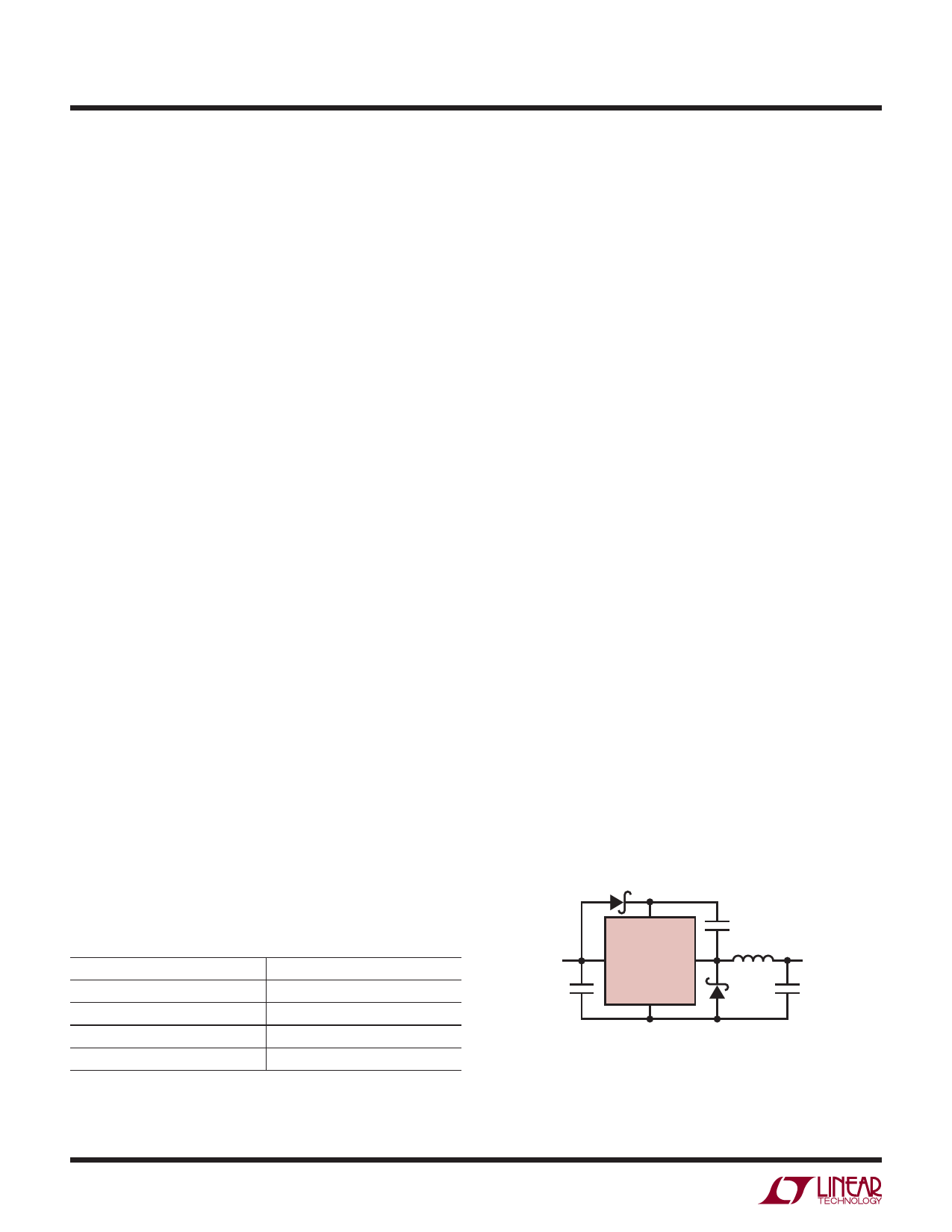
If no voltage supply greater than 2.6V is available, then
an external boost Schottky diode can be tied from the
VIN pin (anode) to the BOOST pin (cathode) as shown in
Figure 3. In this configuration, the BOOST capacitor will be
charged to approximately the VIN voltage, and will change
if VIN changes. In this configuration the maximum operat-
ing VIN is 25V, because when VIN = 25V, then when the
power switch Q1 turns on, VSW ~ 25V, and since the boost
capacitor is charged to 25V, the BOOST pin will be at 50V.
This connection is not as efficient as the others because
the BOOST pin current comes from a higher voltage.
The minimum operating voltage of an LT3645 application
is limited by the undervoltage lockout (~3.4V) and by
the maximum duty cycle as outlined above. For proper
startup, the minimum input voltage is also limited by the
D2
BOOST
C3
LT3645
VIN
VIN
SW
GND
VBOOST – VSW % VIN
MAX VBOOST % 2VIN
Figure 3.
VOUT
3645 F03
3645f
12
Share Link: 