LT3798EMSE 查看數據表(PDF) - Linear Technology
零件编号
产品描述 (功能)
比赛名单
LT3798EMSE Datasheet PDF : 20 Pages
| |||
LT3798
OPERATION
fundamental frequency of the supply voltage is 120Hz so
the control loop unity gain frequency needs to be set less
than approximately 12Hz. Without a large amount of energy
storage on the secondary side, the output current will be
affected by the supply voltage changes, but the DC com-
ponent of the output current will be accurate. For DC input
or non-PFC AC input applications, connect a 25k resistor
from VIN_SENSE to INTVCC instead of the AC line voltage.
Startup
The LT3798 uses a hysteretic start-up to operate from
high offline voltages. A resistor connected to the supply
voltage protects the part from high voltages. This resistor
is connected to the VIN pin on the part and bypassed with
a capacitor. When the resistor charges the VIN pin to a
turn-on voltage set with the EN/UVLO resistor divider and
the INTVCC pin is at its regulation point, the part begins
to switch. The resistor cannot provide power for the part
in steady state, but relies on the capacitor to start-up the
part, then the third winding begins to provide power to the
VIN pin along with the resistor. An internal voltage clamp
is attached to the VIN pin to prevent the resistor current
from allowing VIN to go above the absolute maximum
voltage of the pin. The internal clamp is set at 40V and is
capable of 8mA(typical) of current at room temperature.
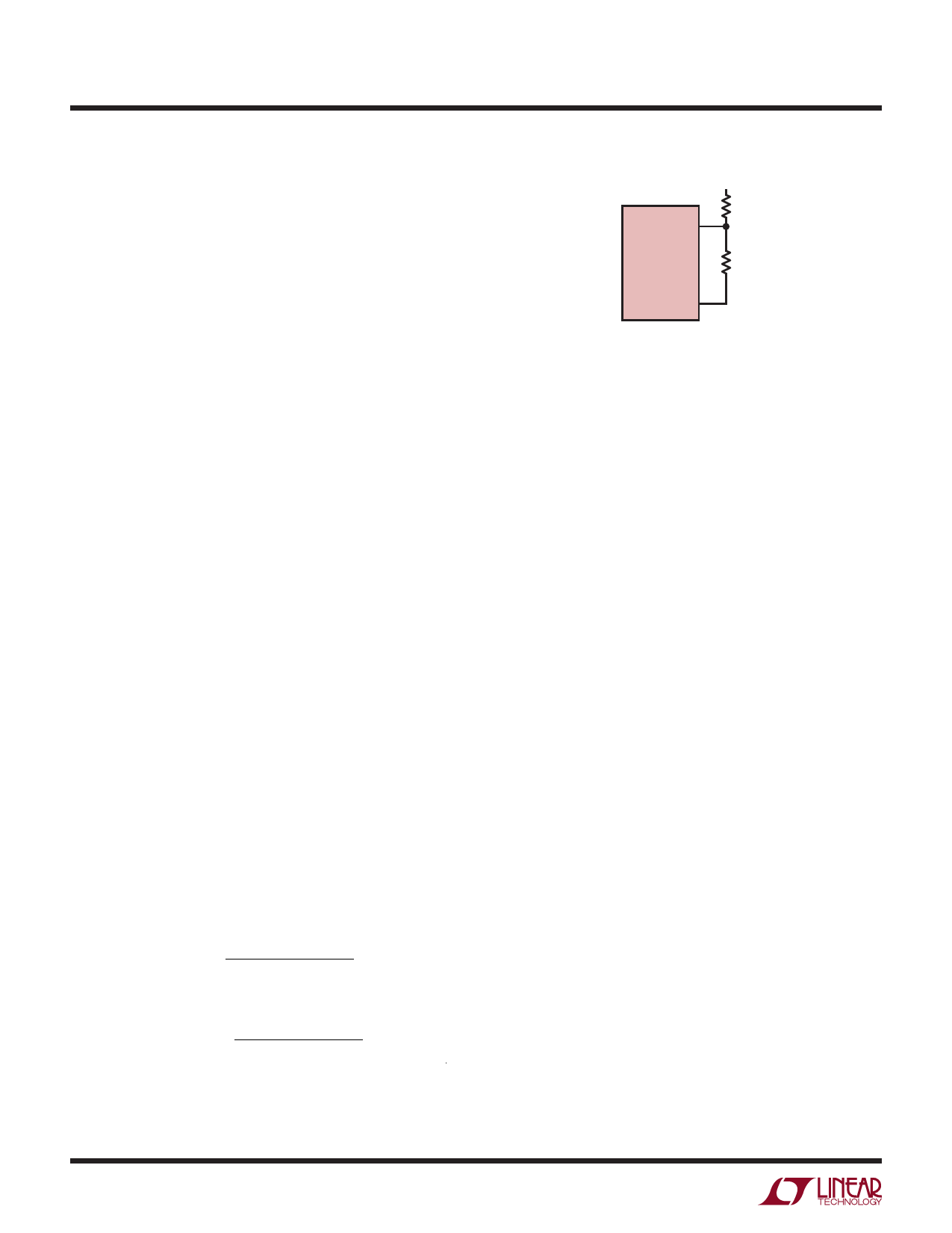
Setting the VIN Turn-On and Turn-Off Voltages
A large voltage difference between the VIN turn-on voltage
and the VIN turn-off voltage is preferred to allow time for the
third winding to power the part. The EN/UVLO sets these
two voltages. The pin has a 10µA current sink when the
pins voltage is below 1.25V and 0µA when above 1.25V.
The VIN pin connects to a resistor divider as shown in
Figure 2. The UVLO threshold for VIN rising is:
VI N(U V L O,R I S I N G)
=
1.25V
• (R1+
R2
R2)
+
10µA
• R1
The UVLO Threshold for VIN Falling is :
VI N(U V L O,F A L L I N G)
=
1.25V
• (R1+
R2
R2)
EN/UVLO
VIN
R1
LT3798
R2
GND
3798 F02
Figure 2. Undervoltage Lockout (UVLO)
Programming Output Voltage
The output voltage is set using a resistor divider from
the third winding to the FB pin. From the Block Diagram,
the resistors R4 and R5 form a resistor divider from the
third winding. The FB also has an internal current source
that compensates for the diode drop. This current source
causes an offset in the output voltage that needs to be ac-
counted for when setting the output voltage. The output
voltage equation is:
VOUT = VBG (R4+R5)/(NST • R5)–(VF + (R4 • ITC)/NST)
where VBG is the internal reference voltage, NST is the
winding ratio between the secondary winding and the third
winding, VF is the forward drop of the output rectifying
diode, and ITC is the internal current source for the FB pin.
The temperature coefficient of the diode's forward drop
needs to be the opposite of the term, (R4 • ITC)/NST. By
taking the partial derivative with respect to temperature,
the value of R4 is found to be the following:
R4 = NST(1/(δITC/δT)(δVF/δT))
δITC/δT = 12.4nA/°C
ITC = 4.25µA
where δITC/δT is the partial derivative of the ITC current
source, and δVF/δT is the partial derivative of the forward
drop of the output rectifying diode.
With R4 set with the above equation, the resistor value
for R5 is found using the following:
R5 = (VBG • R4)/(NST(VOUT+VF)+R4 • ITC-VBG)
3798fa
10
Share Link: 