LT3798IMSE-PBF 查看數據表(PDF) - Linear Technology
零件编号
产品描述 (功能)
比赛名单
LT3798IMSE-PBF Datasheet PDF : 20 Pages
| |||
LT3798
OPERATION
Primary Side Current Control Loop
The CTRL1/CTRL2/CTRL3 pins control the output current
of the flyback controller. To simplify the loop, let’s assume
the VIN_SENSE pin is held at a constant voltage above 1V
eliminating the multiplier from the control loop. The error
amplifier, A5, is configured as integrator with the external
capacitor C6. The COMP+ node voltage is converted to a
current into the multiplier with the V/I converter, A6. Since
A7’s output is constant, the output of the multiplier is
proportional to A6 and can be ignored. The output of the
multiplier controls the peak current with its connection to
the current comparator, A1. The output of the multiplier is
also connected to the transmission gate, SW1, and to a
1M resistor. The transmission gate, SW1, turns on when
the secondary current flows to the output capacitor. This
is called the flyback period when the output diode D1 is
on. The current through the 1M resistor gets integrated by
A5. The lowest CTRL input is equal to the negative input
of A5 in steady state.
A current output regulator normally uses a sense resistor
in series with the output current and uses a feedback loop
to control the peak current of the switching converter. In
this isolated case, the output current information is not
available so instead the LT3798 calculates it using the in-
formation available on the primary side of the transformer.
The output current may be calculated by taking the average
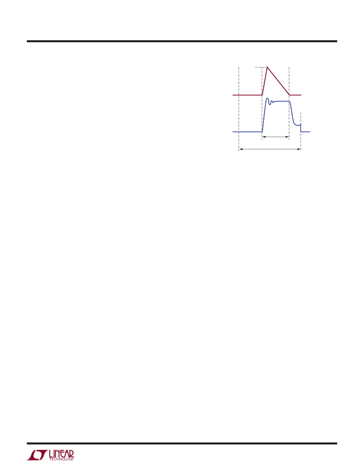
of the output diode current. As shown in Figure 1, the diode
current is a triangle waveform with a base of the flyback
time and a height of the peak secondary winding current.
In a flyback topology, the secondary winding current is N
times the primary winding current, where NPS is the primary
to secondary winding ratio. Instead of taking the area of
the triangle, let’s think of it as a pulse width modulation
(PWM) waveform. During the flyback time, the average
current is half the peak secondary winding current and
zero during the rest of the cycle. The equation to express
the output current is:
IOUT = 0.5 • IPK • NPS • D
where D is equal to the percentage of the cycle that the
flyback time represents. The LT3798 has access to the
primary winding current, the input to the current com-
parator, and when the flyback time starts and ends. Now
the output current can be calculated by averaging a PWM
SECONDARY
DIODE CURRENT
IPK(sec)
SWITCH
WAVEFORM
TFLYBACK
TPERIOD
3798 F01
Figure 1. Secondary Diode Current and Switch Waveforms
waveform with a height of the current limit and a duty cycle
of the flyback time over the entire cycle. In the feedback
loop described above, the input to the integrator is such
a waveform. The integrator adjusts the peak current until
calculated output current equals the control voltage. If the
calculated output current is low compared to the control
pin, the error amplifier increases the voltage on the COMP+
node thus increasing the current comparator input.
Primary Side Voltage Control
The output voltage is available through the third winding on
the primary side. A resistor divider attenuates the output
voltage for the voltage error amplifier. A sample-and-hold
circuit samples the attenuated output voltage and feeds
it to the error amplifier. The output of the error amplifier
is the V pin. This node needs a capacitor to compensate
the output voltage control loop.
Power Factor Correction
When the VIN_SENSE voltage is connected to a resistor divider
of the supply voltage, the current limit is proportional to
the supply voltage. The minimum of the two error ampli-
fier outputs is multiplied with the VIN_SENSE pin voltage. If
the LT3798 is configured with a fast control loop, slower
changes from the VIN_SENSE pin would not interfere with
the current limit or the output current. The COMP+ pin
would adjust to the changes of the VIN_SENSE. The only
way for the multiplier to function is to set the control loop
to be an order of magnitude slower than the fundamental
frequency of the VIN_SENSE signal. In an offline case, the
3798fa
9
Share Link: 