LTC4075HVXEDD 查看數據表(PDF) - Linear Technology
零件编号
产品描述 (功能)
比赛名单
LTC4075HVXEDD Datasheet PDF : 16 Pages
| |||
LTC4075HVX
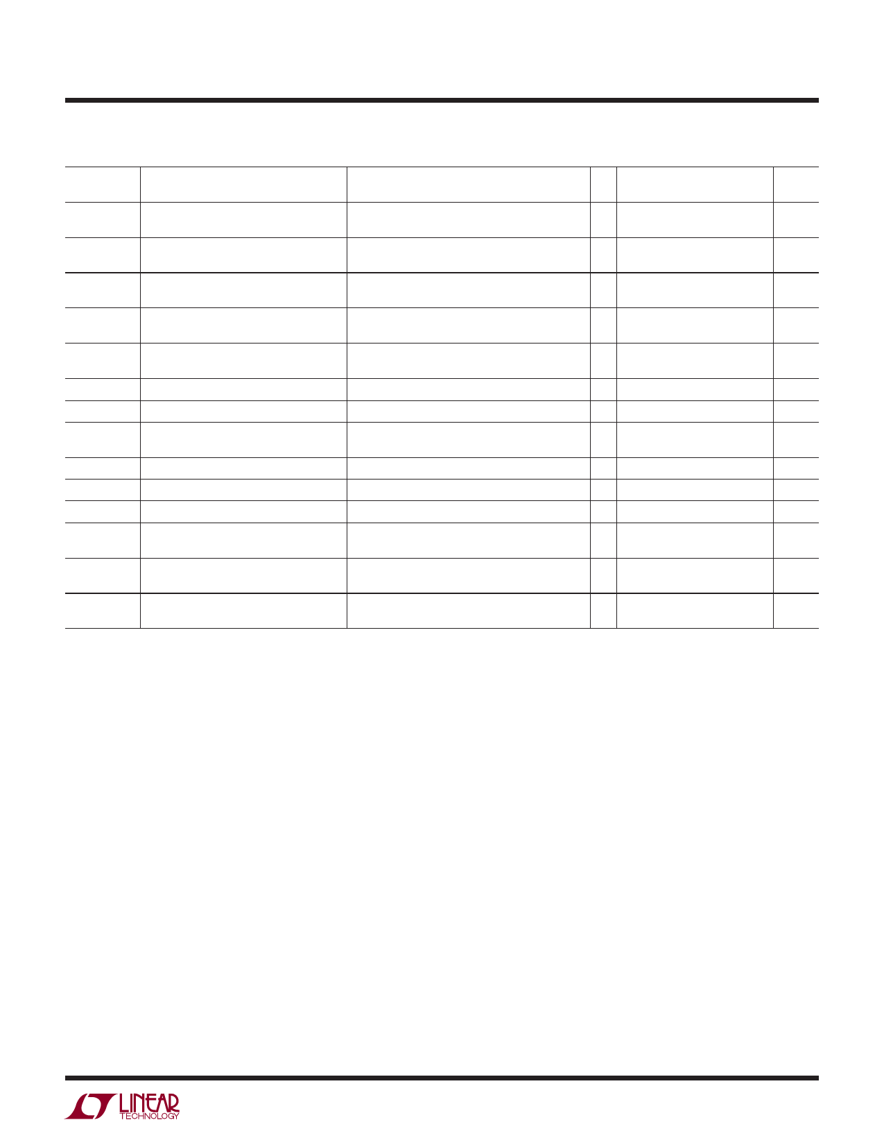
ELECTRICAL CHARACTERISTICS The ● denotes the specifications which apply over the full operating
temperature range, otherwise specifications are at TA = 25°C. VDCIN = 5V, VUSBIN = 5V unless otherwise noted.
VUVDC
VUVUSB
VOVDC
VOVUSB
VASD-DC
VASD-USB
VENABLE
RENABLE
VOL
ΔVRECHRG
tRECHRG
tTERMINATE
RON-DC
RON-USB
TLIM
DCIN Undervoltage Lockout Voltage
USBIN Undervoltage Lockout Voltage
DCIN Overvoltage Lockout Voltage
USBIN Overvoltage Lockout Voltage
VDCIN – VBAT Lockout Threshold
VUSBIN – VBAT Lockout Threshold
ENABLE Input Threshold Voltage
ENABLE Pulldown Resistance
Output Low Voltage
(⎯C⎯H⎯R⎯G, ⎯P⎯W⎯R, USBPWR)
Recharge Battery Threshold Voltage
Recharge Comparator Filter Time
Termination Comparator Filter Time
Power FET “ON” Resistance
(Between DCIN and BAT)
Power FET “ON” Resistance
(Between USBIN and BAT)
Junction Temperature in Constant-
Temperature Mode
From Low to High
Hysteresis
From Low to High
Hysteresis
From Low to High
Hysteresis
From Low to High
Hysteresis
VDCIN from Low to High, VBAT = 4.2V
VDCIN from High to Low, VBAT = 4.2V
VUSBIN from Low to High
VUSBIN from High to Low
ISINK = 5mA
VFLOAT – VRECHRG, 0°C < TA < 85°C
VBAT from High to Low
IBAT Drops Below Termination Threshold
4
4.15
4.3
V
190
mV
3.8
3.95
4.1
V
170
mV
5.8
6
6.2
V
185
mV
5.8
6
6.2
V
185
mV
70
120
170
mV
10
40
70
mV
70
120
170
mV
10
40
70
mV
0.6
0.9
1.2
V
●
1
2
3.5
MΩ
0.12 0.35
V
90
125
160
mV
2.25
4.1
6.75
ms
1
1.6
2.4
ms
600
mΩ
700
mΩ
125
°C
Note 1: Stresses beyond those listed under Absolute Maximum Ratings
may cause permanent damage to the device. Exposure to any Absolute
Maximum Rating condition for extended periods may affect device
reliability and lifetime.
Note 2: The LTC4075HVX is guaranteed to meet the performance
specifications from 0°C to 85°C. Specifications over the –40°C to 85°C
operating temperature range are assured by design, characterization and
correlation with statistical process controls.
Note 3: Failure to correctly solder the exposed backside of the package to
the PC board will result in a thermal resistance much higher than 40°C/W.
See Thermal Considerations.
Note 4: Supply current includes IDC and ITERM pin current (approximately
100μA each) but does not include any current delivered to the battery
through the BAT pin.
Note 5: Supply current includes IUSB and ITERM pin current
(approximately 100μA each) but does not include any current delivered to
the battery through the BAT pin.
4075hvxf
3
Share Link: 