LC75742W 查看數據表(PDF) - SANYO -> Panasonic
零件编号
产品描述 (功能)
比赛名单
LC75742W Datasheet PDF : 18 Pages
| |||
Key input
(KS6 line)
Key scan
LC75742E, LC75742W
Serial data transfer Serial data transfer Key address (8FH) Serial data transfer
Key address
Key data read request
Key data read
Key data read
Key data read request
Multiple Key Presses
The LC75742E/W, even without diodes in the key scan lines, can scan for any combination of dual key presses, any
combination of triple key presses on any of the KI1 to KI5 key scan input pin lines, or any combination of multiple key
presses on any of the KS1 to KS6 key scan output lines. However, keys that are not pressed may be seen as having been
pressed for any other multiple key press combination. Accordingly, applications must insert diodes at each key. Also, to
reject any triple and higher multiple key presses, if three or more data readout are 1 ignore the data by the software or in
other ways.
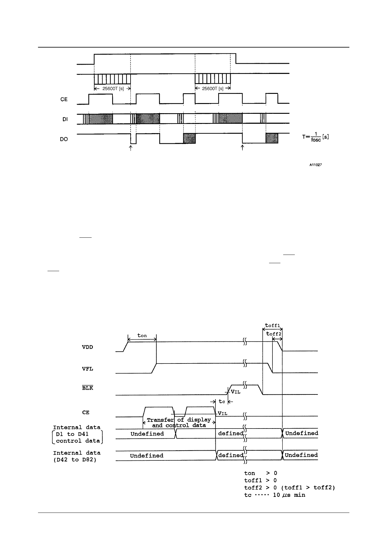
Notes on the BLK Pin and Display Control
Since the states of the IC internal data (D1 to D82, and the control data) are undefined when power is first applied,
applications should turn off the display (i.e. set S1 to S41, and G1 and G2 low) by setting the BLK pin low at the same
time as power is applied. Applications should transfer all 128 bits of the serial data while BLK is held low, and only then
set BLK high. This will prevent random meaningless display at power on. (See figure 4.)
Note on the Power on Sequence
Applications must observe the following sequences when turning the power on or off.
• At power on: First turn on the logic system power (VDD), and then turn on the driver power (VFL)
• At power off: First turn off the driver power (VFL), and then turn off the logic system power (VDD).
Figure 4
No. 6142-11/18
Share Link: 