M34513E4SP/FP 查看數據表(PDF) - Renesas Electronics
零件编号
产品描述 (功能)
比赛名单
M34513E4SP/FP Datasheet PDF : 97 Pages
| |||
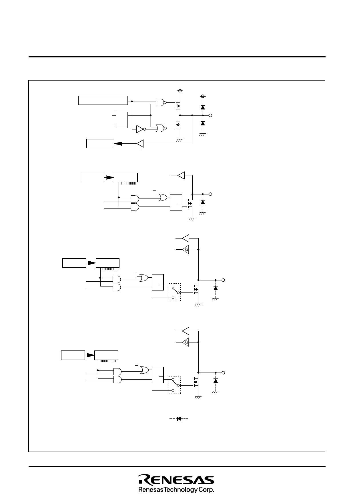
PORT BLOCK DIAGRAMS (continued)
Direction register FR0i
Ai D Q
OP5A instruction T
Register A
IAP5 instruction
Register Y
SD instruction
RD instruction
Decoder Skip decision
(SZD instruction)
CLD instruction
S
RQ
MITSUBISHI MICROCOMPUTERS
4513/4514 Group
SINGLE-CHIP 4-BIT CMOS MICROCOMPUTER
P50–P53
D0–D5
Skip decision (SZD instruction)
Clock input for timer 2 event count
Register Y
Decoder
SD instruction
RD instruction
CLD instruction
S
RQ
W60
0
Timer 1 underflow signal divided by 2 or
1
signal of AND operation between
timer 1 underflow signal divided by 2 and
timer 2 underflow signal divided by 2
D6/CNTR0
Skip decision (SZD instruction)
Clock input for timer 4 event count
Register Y
Decoder
SD instruction
RD instruction
CLD instruction
S
RQ
W62
0
Timer 3 underflow signal divided by 2 or
1
signal of AND operation between
timer 3 underflow signal divided by 2 and
timer 4 underflow signal divided by 2
D7/CNTR1
•
This symbol represents a parasitic diode on the port.
• Applied potential to ports D0–D7 must be 12 V.
• i represents 0, 1, 2, or 3.
• The 4513 Group does not have port P5.
13
Share Link: 