M38C88EA-XXXFP 查看數據表(PDF) - MITSUBISHI ELECTRIC
零件编号
产品描述 (功能)
比赛名单
M38C88EA-XXXFP Datasheet PDF : 51 Pages
| |||
PRELIMINARY NSocothimcaene:gpTeah.riasmisetnrioct laimfiintsalasrepescuibfijceacttioton.
MITSUBISHI MICROCOMPUTERS
38C8 Group
SINGLE-CHIP 8-BIT CMOS MICROCOMPUTER
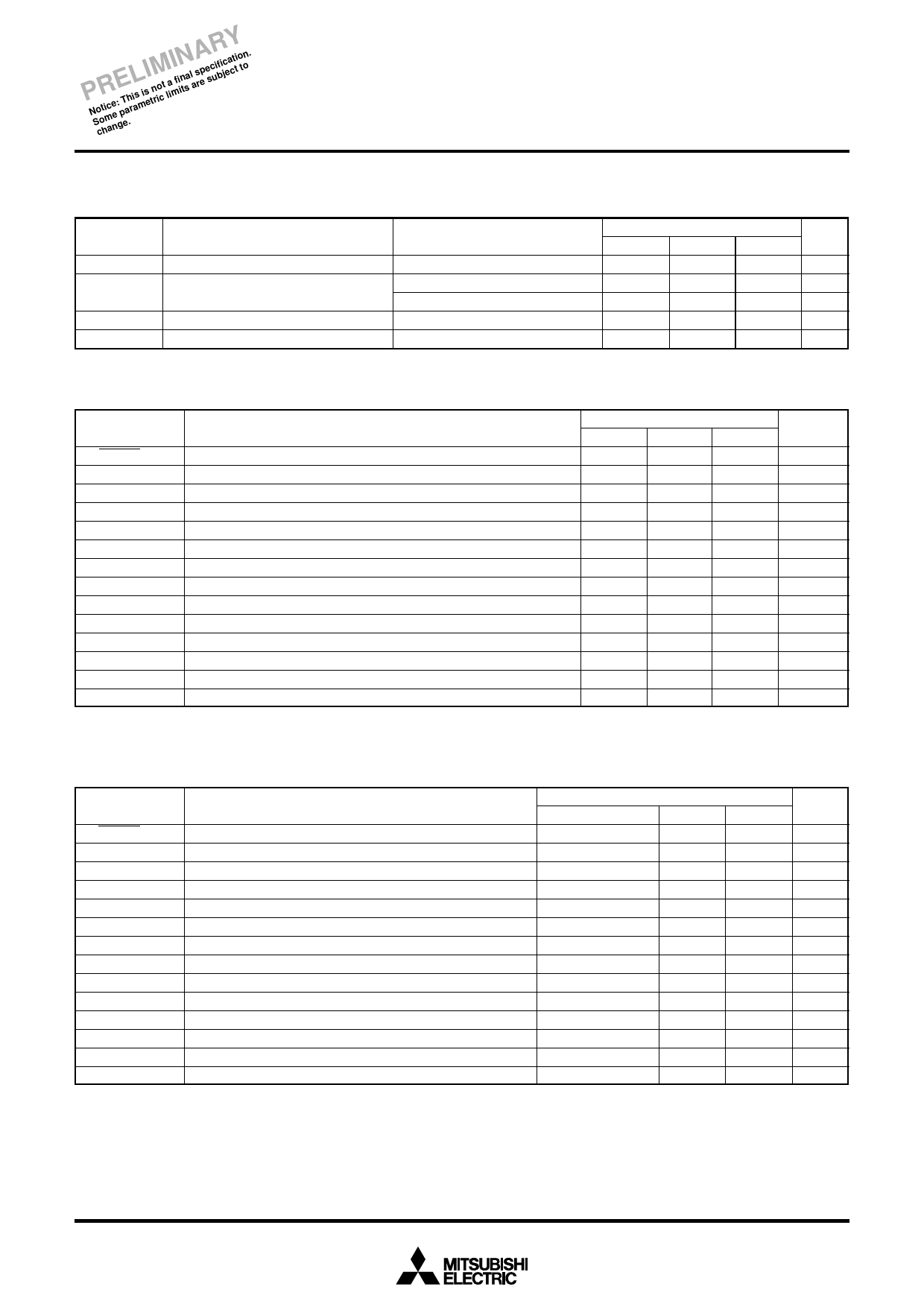
Table 16 A-D converter characteristics
(Vcc = 2.2 to 5.5 V, Vss = 0 V, Ta = –20 to 85°C, f(XIN) ≤ 4 MHz, in middle-speed/high-speed mode)
Symbol
Parameter
—
—
tconv
IIA
Resolution
Absolute accuracy
(excluding quantization error)
Conversion time
Analog port input current
Note: When main clock is selected as system clock.
Test conditions
Min.
VCC = 2.7–5.5 V
VCC = 2.5–2.7 V (Ta = –10 to 50 °C)
f(XIN) = 4 MHz (Note)
30.5
Limits
Typ.
0.5
Unit
Max.
10
Bits
±4
LSB
±6
LSB
34
µs
5.0
µA
Table 17 Timing requirements 1 (Vcc = 4.0 to 5.5 V, Vss = 0 V, Ta = –20 to 85°C, unless otherwise noted)
Symbol
Parameter
tw(RESET)
Reset input “L” pulse width
tc(XIN)
Main clock input cycle time (XIN input)
twH(XIN)
Main clock input “H” pulse width
twL(XIN)
Main clock input “L” pulse width
tc(CNTR)
CNTR0, CNTR1 input cycle time
twH(CNTR)
CNTR0, CNTR1 input “H” pulse width
twL(CNTR)
CNTR0, CNTR1 input “L” pulse width
twH(INT)
INT0, INT1 input “H” pulse width
twL(INT)
INT0, INT1 input “L” pulse width
tc(SCLK)
Serial I/O clock input cycle time
twH(SCLK)
Serial I/O clock input “H” pulse width
twL(SCLK)
Serial I/O clock input “L” pulse width
tsu(RxD-SCLK)
Serial I/O input setup time
th(SCLK-RxD)
Serial I/O input hold time
Note: When bit 6 of address 001A16 is “1”.
Divide this value by four when bit 6 of address 001A16 is “0”.
(Note)
(Note)
(Note)
Limits
Unit
Min.
Typ.
Max.
2
µs
125
ns
45
ns
40
ns
250
ns
105
ns
105
ns
80
ns
80
ns
800
ns
370
ns
370
ns
220
ns
100
ns
Table 18 Timing requirements 2 (Vcc = 2.2 to 4.0 V, Vss = 0 V, Ta = –20 to 85°C, unless otherwise noted)
Symbol
Parameter
tw(RESET)
Reset input “L” pulse width
tc(XIN)
Main clock input cycle time (XIN input)
twH(XIN)
Main clock input “H” pulse width
twL(XIN)
Main clock input “L” pulse width
tc(CNTR)
CNTR0, CNTR1 input cycle time
twH(CNTR)
CNTR0, CNTR1 input “H” pulse width
twL(CNTR)
CNTR0, CNTR1 input “L” pulse width
twH(INT)
NT0, INT1 input “H” pulse width
twL(INT)
NT0, INT1 input “L” pulse width
tc(SCLK)
Serial I/O clock input cycle time
twH(SCLK)
Serial I/O clock input “H” pulse width
twL(SCLK)
Serial I/O clock input “L” pulse width
tsu(RxD-SCLK)
Serial I/O input setup time
th(SCLK-RxD)
Serial I/O input hold time
Note: When bit 6 of address 001A16 is “1”.
Divide this value by four when bit 6 of address 001A16 is “0”.
(Note)
(Note)
(Note)
Limits
Min.
Typ.
2
125
45
40
900/(VCC–0.4)
tc(CNTR)/2–20
tc(CNTR)/2–20
230
230
2000
950
950
400
200
Unit
Max.
µs
ns
ns
ns
ns
ns
ns
ns
ns
ns
ns
ns
ns
ns
46
Share Link: 