M51945A 查看數據表(PDF) - Renesas Electronics
零件编号
产品描述 (功能)
比赛名单
M51945A Datasheet PDF : 11 Pages
| |||
M51945A,B/M51946A,B
Notice for use
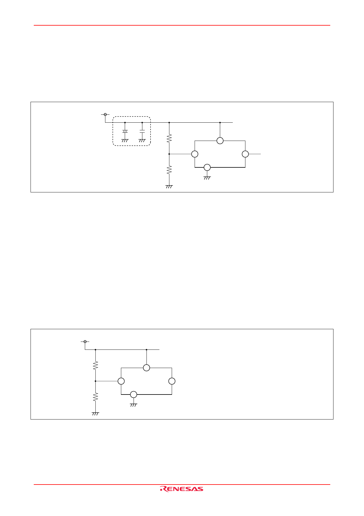
About the Power Supply Line
1. About bypass capacitor
Because the ripple and the spike of the high frequency noise and the low frequency are superimposed to the power
supply line, it is necessary to remove these.
Therefore, please install C1 and C2 for the low frequency and for the high frequency between the power supply line
and the GND line as shown in following figure 2.
VCC
C1+ C2
R1
Example of ripple
noise measures
Vin
R2
Input
Power-supply
M51945
M51946
Output
GND
Figure 2 Example of Ripple Noise Measures
2. The sequence of voltage impression
Please do not impress the voltages to the input terminals earlier than the power supply terminal. Moreover, please
do not open the power supply terminal with the voltage impressed to the input terminal.
(The setting of the bias of an internal circuit collapses, and a parasitic element might operate.)
About the Input Terminal
1. Setting range of input voltage
The following voltage is recommended to be input to the input terminal (pin 2).
about 0.8 (V) < Vin < VCC – 0.3 (V) .... at VCC ≤ 7 V
about 0.8 (V) < Vin < 6.7 (V) .............. at VCC > 7 V
2. About using input terminal
Please do an enough verification to the transition characteristic etc. of the power supply when using independent
power supply to input terminal (pin 2).
VCC
Vin
Input
Vin is decided to the VCC subordinating,
Power-supply and operates in the range
about 0.8 (V) < Vin < VCC – 0.3 (V).
M51945
Output
M51946
GND
Figure 3 Recommended Example
REJ03D0774-0200 Rev.2.00 Aug 20, 2007
Page 6 of 10
Share Link: 