A62S7332E-5 查看數據表(PDF) - AMIC Technology
零件编号
产品描述 (功能)
比赛名单
A62S7332E-5
AMIC Technology

A62S7332E-5 Datasheet PDF : 17 Pages
| |||
A63G7332 Series
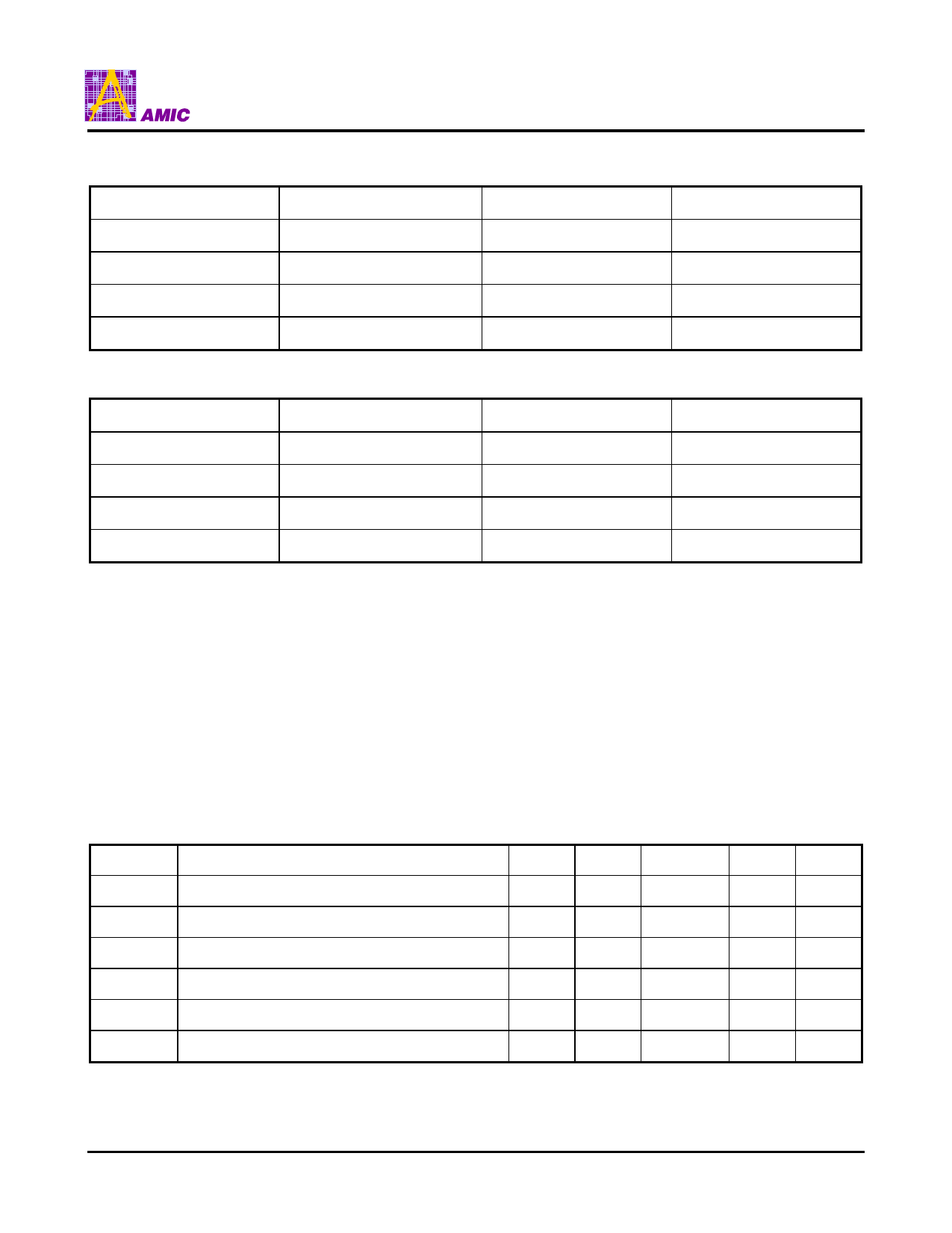
Linear Burst Address Table (MODE = LOW)
First Address (External)
X . . . X00
X . . . X01
X . . . X10
X . . . X11
Second Address (Internal)
X . . . X01
X . . . X10
X . . . X11
X . . . X00
Third Address (Internal) Fourth Address (Internal)
X . . . X10
X . . . X11
X . . . X11
X . . . X00
X . . . X00
X . . . X01
X . . . X01
X . . . X10
Interleaved Burst Address Table (MODE = HIGH or NC)
First Address (External)
X . . . X00
X . . . X01
X . . . X10
X . . . X11
Second Address (Internal)
X . . . X01
X . . . X00
X . . . X11
X . . . X10
Third Address (Internal) Fourth Address (Internal)
X . . . X10
X . . . X11
X . . . X11
X . . . X10
X . . . X00
X . . . X01
X . . . X01
X . . . X00
Absolute Maximum Ratings*
*Comments
Power Supply Voltage (VCC) . . . . . . . . . . -0.5V to +4.6V
Voltage Relative to GND for any Pin Except VCC (Vin,
Vout) . . . . . . . . . . . . . . . . . . . . . . . . . -0.5V to VCC +0.5V
Power Dissipation (PD) . . . . . . . . . . . . . . . . . . . . . . . . 2W
Operating Temperature (Topr) . . . . . . . . . . . 0°C to 70°C
Storage Temperature (Tbias) . . . . . . . . . . -10°C to 85 °C
Storage Temperature (Tstg) . . . . . . . . . . . -55°C to 125°C
Stresses above those listed under "Absolute Maximum
Ratings" may cause permanent damage to this device.
These are stress ratings only. Functional operation of
this device at these or any other conditions above those
indicated in the operational sections of this specification
is not implied or intended. Exposure to the absolute
maximum rating conditions for extended periods may
affect device reliability.
Recommended DC Operating Conditions
(0°C ≤ TA ≤ 70°C, VCC = 3.3V+10% or 3.3V-5%, VCCQ = +2.5V+0.4V/-0.125V, unless otherwise noted)
Symbol
VCC
VCCQ
GND
VIH
VIHQ
VIL
Parameter
Supply Voltage (Operating Voltage Range)
Isolated Input Buffer Supply
Supply Voltage to GND
Input High Voltage
Input High Voltage
Input Low Voltage
Min.
3.1
2.375
0.0
1.7
1.7
-0.3
Typ.
3.3
2.5
-
-
-
-
Max.
3.6
2.9
0.0
VCC+0.3
VCC+0.3
0.7
Unit
V
V
V
V
V
V
Note
1, 2
1, 2
PRELIMINARY (December, 1998, Version 2.1)
7
AMIC Technology, Inc.
Share Link: