STK730C 查看數據表(PDF) - SANYO -> Panasonic
零件编号
产品描述 (功能)
比赛名单
STK730C Datasheet PDF : 6 Pages
| |||
STK730C θj-c, Tj max
PTR (FET)
FWD (SBD)
θj-c
3.5°C/W
7.2°C/W
Tj max
150°C
125°C
Notes on PC Board Production
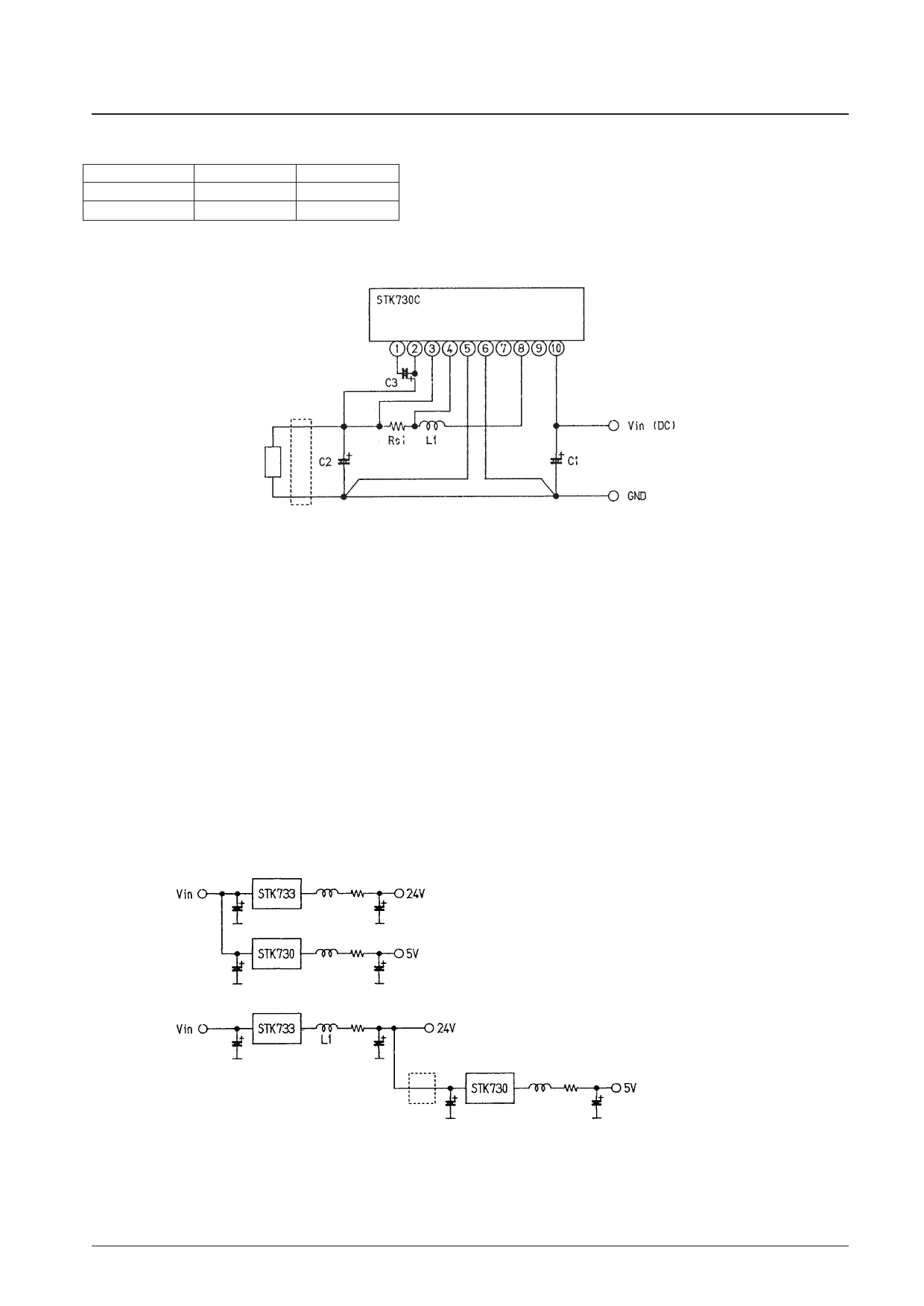
STK730C
• Capacitor C1 should be placed as close as possible to the pin 10 input in the layout. (This is to prevent voltage drops in
the input lines and pattern. Also, a separate smoothing capacitor is required if the input is a direct current input using
rectified and smoothed AC.)
• Capacitor C2 should be placed as close as possible to the load in the layout. (This is to compensate for voltage drops
due to load fluctuations.)
• Pins 2 and 5 are voltage sensing lines, and should be connected close to the load, i.e., close to C2. (This is to
compensate for voltage drops in the pattern.)
• Pins 3 and 4 should be directly connected to the two terminals of the current detection resistor Rs1. (This is to prevent
detection based on pattern resistances.)
• Pin 6 should be connected to the capacitor C1 ground using a thick, short line to reduce the related loop area. (This is
to reduce switching spikes.)
• Power lines, i.e., lines that carry current, should be made as wide as possible in the pattern.
• When a ripple suppression LC filter is added, connect it at the location indicated by dotted lines in the figure. The
sensing line from pin 2 should be connected to the same position (the C2 location) as it is when no filter is used.
• The NC pins (pins 7 and 9) should not be connected to any other lines, even on the PC board.
Two Output Power Supply Structural Example (connecting to an STK733)
Note: It is possible for STK730 input ripple currents to cause L1 to vibrate audibly and adversely influence the 24 V system. If such problems occur, an
inductor can be inserted at the point marked with dotted lines in the figure to form an LC filter.
No. 4472-5/6
Share Link: 