XRD6406 查看數據表(PDF) - Exar Corporation
零件编号
产品描述 (功能)
比赛名单
XRD6406 Datasheet PDF : 12 Pages
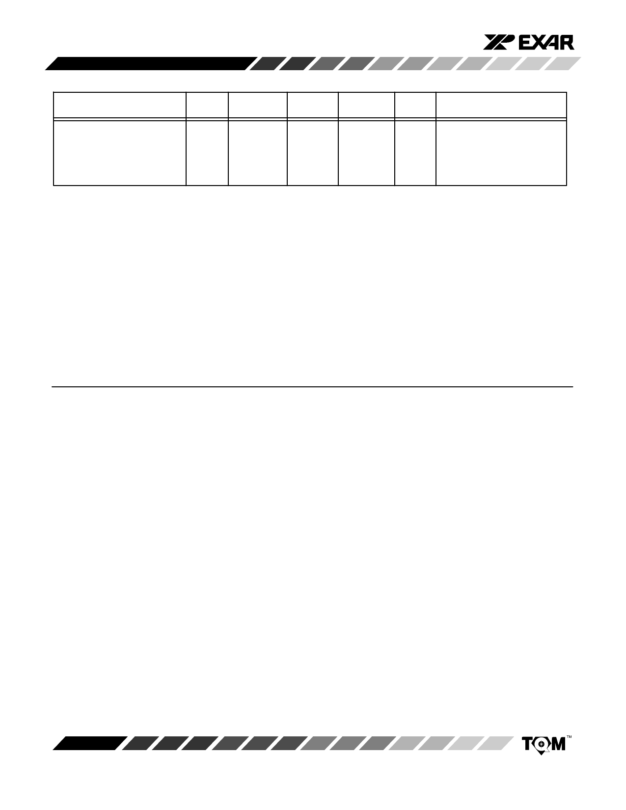
| |||
XRD6406
ELECTRICAL CHARACTERISTICS TABLE (CONT’D)
Description
25°C
Symbol
Min
Typ
Max
POWER SUPPLIES
Operating Voltage
(AVDD, DVDD)8, 9
Current (AVDD + DVDD)
VDD
4.5
5
5.5
IDD
13
17
Units
Conditions
V
mA
Notes:
1 Tester measures code transitions by dithering the voltage of the analog input (VIN). The difference between the measured and the
ideal code width (VREF/1024) is the DNL error (Figure 3.). The INL error is the maximum distance (in LSBs) from the best fit line to
any transition voltage (Figure 4.). Accuracy is a function of the sampling rate (FS).
2 Guaranteed. Not tested.
3 Specified values guarantee functionality, but INL & DNL specifications may not be met.
4 --1 dB bandwidth is a measure of performance of the A/D input stage (S/H + amplifier). Refer to other parameters for accuracy within
the specified bandwidth.
5
6
7
8
TDCAShleVoleenDindDAVpi.tIGuNiotNsneDhqtoau&vimveDaeldGeeitnoNtadDcpeiesprcritntuousirtDea(VFrdeDiegDcluaorayennsn8dpe.e)cD.ctGeiSfdiNcwtDahitt.rcioohInunesgpdhu(ctAttahPDpe,CatsAcicJiltiu)co.rorrAneanncsttausulboawsgl itrlrliiansnetpeo/uf.tateClrlxeotcqimneuneieredeccssatpdntoeribgcveieefitrelhedwesrisltihamstltiottrshiwnefgooperuanatctpnkwuyatitgirhneepnsuaiostntlvdaoonstlocstaetogh.feeabacenctauwlroaegceyng.rDoGunNdDpalannde.
9 The AVDD & DVDD pins should be tied together at the package.
Specifications are subject to change without notice
ABSOLUTE MAXIMUM RATINGS (TA = +25°C unless otherwise noted)1, 2, 3
AVDD to AGND . . . . . . . . . . . . . . . . . . . . . . . . . . . . . . . . . . +7V
VRT & VRB . . . . . . . . . . . . . . . . . . . . . VDD +0.5 to GND --0.5V
VIN . . . . . . . . . . . . . . . . . . . . . . . . . . . VDD +0.5 to GND --0.5V
All Inputs . . . . . . . . . . . . . . . . . . . . . . VDD +0.5 to GND --0.5V
All Outputs . . . . . . . . . . . . . . . . . . . . VDD +0.5 to GND --0.5V
Storage Temperature . . . . . . . . . . . . . . . . . . . --65 to +150°C
Package Power Dissipation Rating to 75°C
PDIP, SOIC . . . . . . . . . . . . . . . . . . . . . . . . . . . . . . . 1000mW
Derates above 75°C . . . . . . . . . . . . . . . . . . . . . . . 14mW/°C
Lead Temperature (Soldering 10 seconds) . . . . . . . +300°C
Notes
1 Stresses above those listed under “Absolute Maximum Ratings” may cause permanent damage to the device. This is a
stress rating only and functional operation at or above this specification is not implied. Exposure to maximum rating
conditions for extended periods may affect device reliability.
2 Any input pin which can see a value outside the absolute maximum ratings should be protected by Schottky diode clamps
(HP5082-2835) from input pin to the supplies. All inputs have protection diodes which will protect the device from short
3
transients outside the supplies of less than 100mA for less than 100ms.
VDD refers to AVDD and DVDD. GND refers to AGND and DGND.
Rev. 1.00
4
Share Link: 