MC07XSC200 查看數據表(PDF) - Freescale Semiconductor
零件编号
产品描述 (功能)
比赛名单
MC07XSC200 Datasheet PDF : 51 Pages
| |||
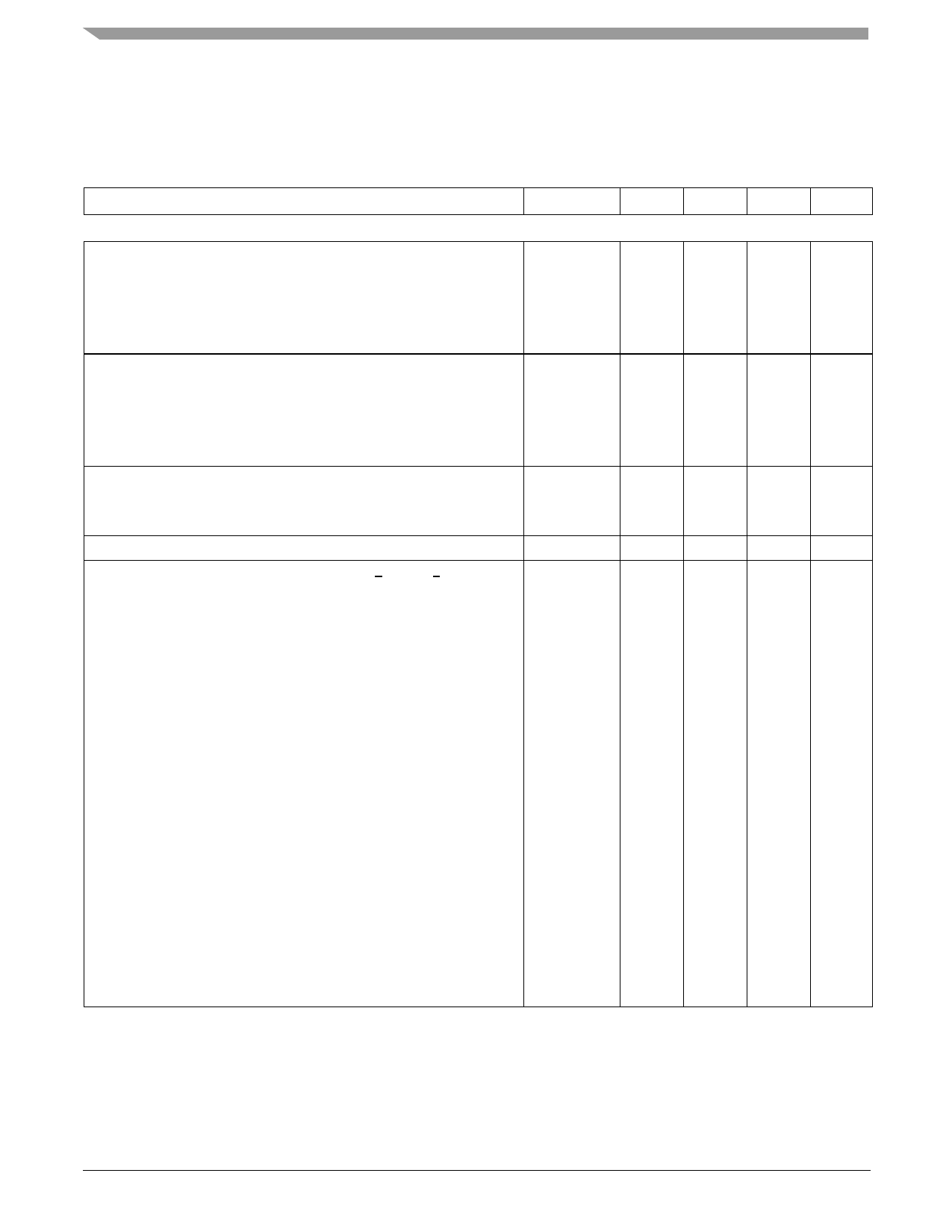
Table 3. Static Electrical Characteristics (continued)
Characteristics noted under conditions 6.0 V VPWR 20 V, 3.0 V VDD 5.5 V, - 40 C TA 125 C, GND = 0 V, unless
otherwise noted. Typical values noted reflect the approximate parameter means at TA = 25 °C under nominal conditions, unless
otherwise noted.
Characteristic
Symbol
Min
Typ
Max
Unit
OUTPUTS HS0 TO HS1
HS[0,1] Output Drain-to-Source ON Resistance (IHS = 5.0 A, TA = 25 C)
• VPWR = 4.5 V
• VPWR = 6.0 V
• VPWR = 10 V
• VPWR = 13 V
RDS_01(ON)
–
–
–
–
m
–
25.2
–
11.2
–
7.0
–
7.0
HS[0,1] Output Drain-to-Source ON Resistance (IHS = 5.0 A, TA = 150 C)
RDS_01(ON)
• VPWR = 4.5 V
–
• VPWR = 6.0 V
–
• VPWR = 10 V
–
• VPWR = 13 V
–
m
–
42.8
–
19.1
–
11.9
–
11.9
HS[0,1] Output Source-to-Drain ON Resistance (IHS = -5.0 A, VPWR= -18 V)(12) RSD_01(ON)
• TA = 25 C
–
• TA = 150 C
–
m
–
10.5
–
14
HS[0,1] Maximum Severe Short-circuit Impedance Detection(13)
RSHORT_01
21
47
75
m
HS[0,1] Output Overcurrent Detection Levels (6.0 V < VHS[0:1] < 20 V)
• 28W bit = 0
A
OCHI1_0
89.9
114.8
139.8
OCHI2_0
67
83.7
100.4
OC1_0
48
61.2
74.4
OC2_0
42
53.2
64.4
OC3_0
35.2
44.6
54
OC4_0
28.8
36.4
44
OCLO4_0
21
26.6
32.1
OCLO3_0
13.3
18.4
23.5
OCLO2_0
11.3
14.2
17.1
OCLO1_0
7.4
9.3
11.2
• 28W bit = 1
OCHI1_1
44.9
57.4
69.9
OCHI2_1
33.5
41.9
50.2
OC1_1
24
30.6
37.2
OC2_1
20.8
26.5
32.1
OC3_1
17.6
22.3
27
OC4_1
14.4
18.2
22
OCLO4_1
6.1
7.6
9.0
OCLO3_1
6.1
7.6
9.0
OCLO2_1
6.1
7.6
9.0
OCLO1_1
2.7
4.9
7.0
Notes
12. Source-Drain ON Resistance (Reverse Drain-to-Source ON Resistance) with negative polarity VPWR.
13. Short-circuit impedance calculated from HS[0:1] to GND pins. Value guaranteed per design.
07XSC200
8
Analog Integrated Circuit Device Data
Freescale Semiconductor
Share Link: 