MC145193 查看數據表(PDF) - Motorola => Freescale
零件编号
产品描述 (功能)
比赛名单
MC145193 Datasheet PDF : 24 Pages
| |||
MC145193
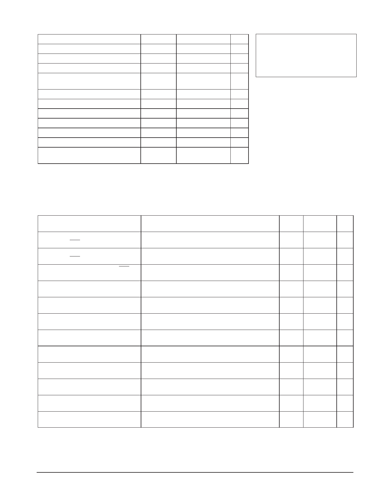
MAXIMUM RATINGS* (Voltages Referenced to Gnd, unless otherwise stated)
Parameter
Symbol
Value
Unit
DC Supply Voltage (Pins 12 and 14)
VCC, VDD
–0.5 to 6.0
V
DC Supply Voltage (Pin 5)
VPD
VDD – 0.5 to 6.0
V
DC Input Voltage
Vin
–0.5 to VDD + 0.5
V
DC Output Voltage (except Output B, PDout,
φR, φV)
Vout
–0.5 to VDD + 0.5
V
DC Output Voltage (Output B, PDout, φR, φV)
Vout
–0.5 to VPD + 0.5
V
DC Input Current, per Pin (Includes VPD)
Iin, IPD
±10
mA
DC Output Current, per Pin
Iout
±20
mA
DC Supply Current, VDD and Gnd Pins
IDD
±30
mA
Power Dissipation, per Package
PD
300
mW
Storage Temperature
Tstg
–65 to 150
°C
Lead Temperature, 1 mm from Case for 10
TL
Seconds
260
°C
NOTES: 1. Maximum Ratings are those values beyond which damage to the device may occur.
Functional operation should be restricted to the limits in the Electrical Characteristics tables or
Pin Descriptions section.
2. ESD (electrostatic discharge) immunity meets Human Body Model (HBM) ≤2000 V and
Machine Model (MM) ≤200 V. Additional ESD data available upon request.
This device contains protection circuitry
to guard against damage due to high static
voltages or electric fields. However, precau-
tions must be taken to avoid applications of
any voltage higher than maximum rated
voltages to this high–impedance circuit.
ELECTRICAL CHARACTERISTICS
(VDD = VCC = 2.7 to 5.5 V, Voltages Referenced to Gnd, unless otherwise stated; VPD = 2.7 to 5.5 V, TA = –40 to 85°C)
Parameter
Test Condition
Guaranteed
Symbol
Limit
Unit
Maximum Low–Level Input Voltage
(Din, CLK, ENB)
Minimum High–Level Input Voltage
(Din, CLK, ENB)
Minimum Hysteresis Voltage (CLK, ENB)
Maximum Low–Level Output Voltage
(REFout, Output A)
Minimum High–Level Output Voltage
(REFout, Output A)
Minimum Low–Level Output Current
(REFout, LD)
Minimum Low–Level Output Current
(φR, φV)
Minimum Low–Level Output Current
(Output A)
Minimum Low–Level Output Current
(Output B)
VDD = 2.7 V
VDD = 4.5 V
Iout = 20 µA, Device in Reference Mode
Iout = – 20 µA, Device in Reference Mode
Vout = 0.3 V
Vout = 0.3 V
Vout = 0.4 V
VDD = 4.5 V
Vout = 0.4 V
VIL
0.3 x VDD V
VIH
0.7 x VDD V
VHys
VOL
100
mV
250
0.1
V
VOH VDD – 0.1 V
IOL
0.36
mA
IOL
0.36
mA
IOL
1.0
mA
IOL
1.0
mA
Minimum High–Level Output Current
(REFout, LD)
Minimum High–Level Output Current
(φR, φV)
Minimum High–Level Output Current
(Output A Only)
Vout = VDD – 0.3 V
Vout = VPD – 0.3 V
Vout = VDD – 0.4 V
VDD = 4.5 V
IOH
–0.36
mA
IOH
–0.36
mA
IOH
–0.6
mA
(continued)
MOTOROLA WIRELESS SEMICONDUCTOR
3
SOLUTIONS – RF AND IF DEVICE DATA
Share Link: 