MC74VHCT245A 查看數據表(PDF) - ON Semiconductor
零件编号
产品描述 (功能)
比赛名单
MC74VHCT245A Datasheet PDF : 7 Pages
| |||
MC74VHCT245A
Octal Bus Transceiver
The MC74VHCT245A is an advanced high speed CMOS octal bus
transceiver fabricated with silicon gate CMOS technology. It achieves
high speed operation similar to equivalent Bipolar Schottky TTL
while maintaining CMOS low power dissipation.
It is intended for two−way asynchronous communication between
data buses. The direction of data transmission is determined by the
level of the DIR input. The output enable pin (OE) can be used to
disable the device, so that the buses are effectively isolated.
All inputs are equipped with protection circuits against static
discharge.
The VHCT inputs are compatible with TTL levels. This device can
be used as a level converter for interfacing 3.3 V to 5.0 V, because it
has full 5.0 V CMOS level output swings.
The VHCT245A input and output (when disabled) structures
provide protection when voltages between 0 V and 5.5 V are applied,
regardless of the supply voltage. These input and output structures
help prevent device destruction caused by supply
voltage−input/output voltage mismatch, battery backup, hot insertion,
etc.
Features
• High Speed: tPD = 4.9 ns (Typ) at VCC = 5.0 V
• Low Power Dissipation: ICC = 4 mA (Max) at TA = 25°C
• TTL−Compatible Inputs: VIL = 0.8 V; VIH = 2.0 V
• Power Down Protection Provided on Inputs and Outputs
• Balanced Propagation Delays
• Designed for 4.5 V to 5.5 V Operating Range
• Low Noise: VOLP = 1.6 V (Max)
• Pin and Function Compatible with Other Standard Logic Families
• Latchup Performance Exceeds 300 mA
• ESD Performance:
Human Body Model > 2000 V;
Machine Model > 200 V
• Chip Complexity: 304 FETs or 76 Equivalent Gates
• Pb−Free Packages are Available*
APPLICATION NOTES
• Do not force a signal on an I/O pin when it is an active output,
damage may occur.
• All floating (high impedance) input or I/O pins must be fixed by
means of pullup or pulldown resistors or bus terminator ICs.
http://onsemi.com
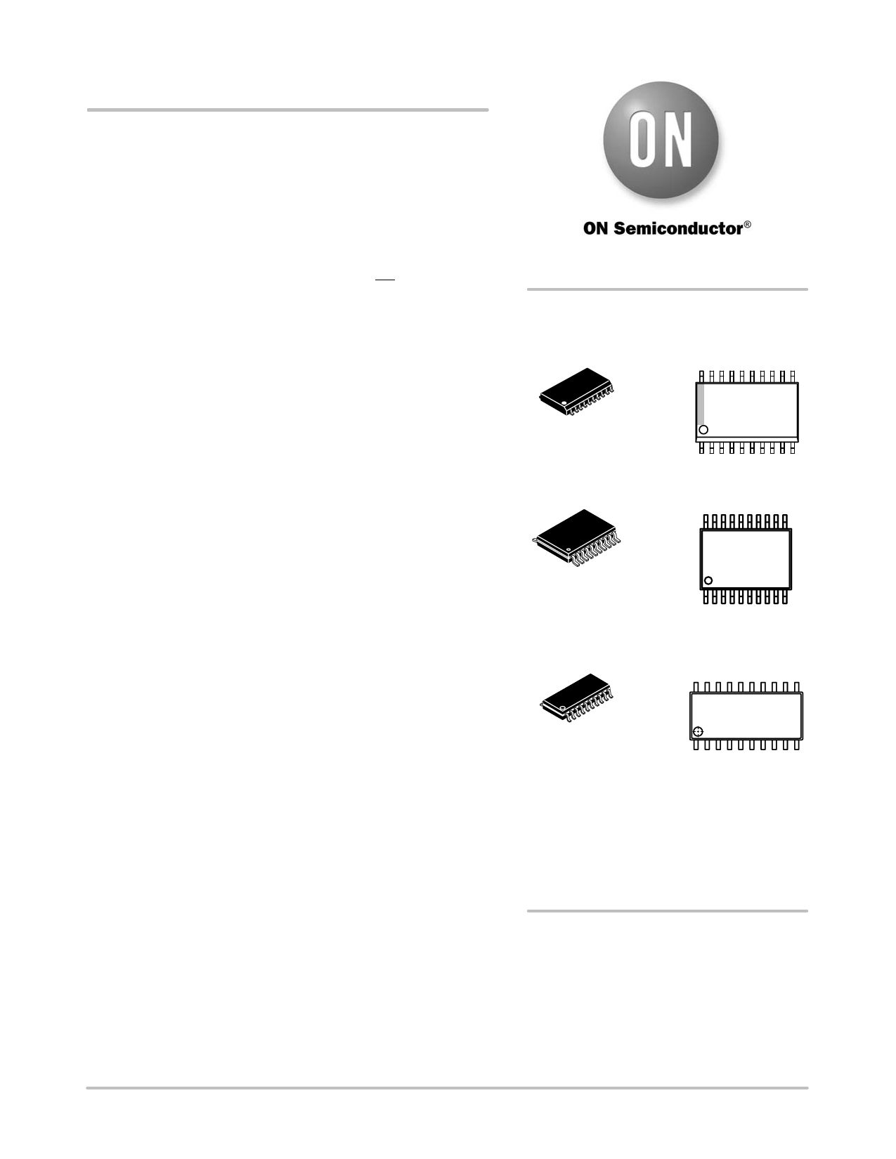
MARKING
DIAGRAMS
20
VHCT245A
1 SOIC−20WB
SUFFIX DW
AWLYYWWG
CASE 751D 1
20
1 TSSOP−20
SUFFIX DT
CASE 948E 1
VHCT
245A
ALYWG
G
20
74VHCT245
SOEIAJ−20
AWLYWWG
1
SUFFIX M
CASE 967 1
A
= Assembly Location
WL, L = Wafer Lot
YY, Y = Year
WW, W = Work Week
G or G = Pb−Free Package
(Note: Microdot may be in either location)
ORDERING INFORMATION
See detailed ordering and shipping information in the package
dimensions section on page 4 of this data sheet.
*For additional information on our Pb−Free strategy and soldering details, please
download the ON Semiconductor Soldering and Mounting Techniques
Reference Manual, SOLDERRM/D.
© Semiconductor Components Industries, LLC, 2006
1
January, 2006 − Rev. 5
Publication Order Number:
MC74VHCT245A/D
Share Link: 